
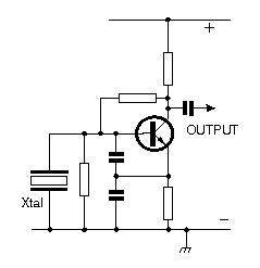
Butler emitter follower oscillator

The circuit in question utilizes series resonance to achieve optimal performance. At series resonance, the inductive and capacitive reactances are equal in magnitude but opposite in phase, resulting in a purely resistive impedance. This characteristic allows for maximum current flow through the circuit at the resonant frequency, making it highly efficient for applications such as RF signal processing and filtering.
The absence of parasitic elements is a significant advantage, as parasitics can introduce unwanted losses and distortions that degrade circuit performance. This circuit's design minimizes these effects, ensuring that the desired signal characteristics are preserved.
Tuning the circuit is facilitated by adjustable components, such as variable capacitors or inductors, which enable precise control over the resonant frequency. This feature is particularly beneficial in applications where frequency adjustments are necessary, such as in oscillators or tunable filters.
Moreover, the circuit exhibits good frequency stability, which is crucial for maintaining consistent performance over time and varying operating conditions. Stability is often enhanced through careful component selection and layout design, reducing susceptibility to temperature variations and other environmental factors.
Overall, this circuit design is suitable for a range of applications requiring reliable performance at or near resonance, combining ease of tuning with robust frequency stability.This circuit operates at or near series resonance. It is a good circuit design with no parasitics It is easy to tune with good frequency stability.
Related Circuits

This is a circuit known as a Wien bridge oscillator. The circuit features both positive and negative feedback loops and operates under the control of an operational amplifier (op-amp). The oscillation frequency is determined by the RC time constant,...
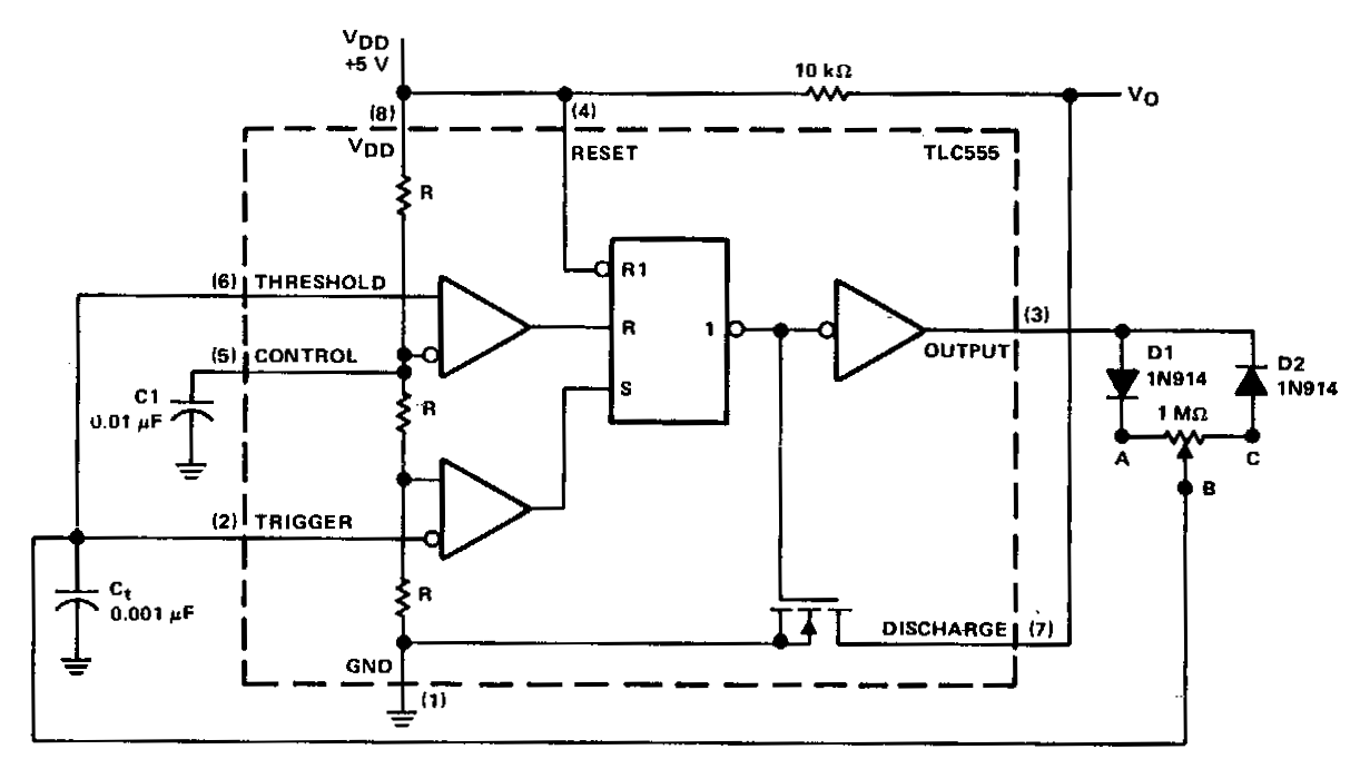
In a basic astable timer, the timing periods 11 and 12 are not independently controlled. This lack of control complicates the maintenance of a constant period, T, if either 11 or 12 is varied. In this circuit, the charge...
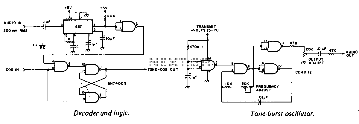
A tone burst sent at the beginning of each transmission is decoded at the receiver by a phase-locked loop (PLL), resulting in an output from pin 3 of a logic gate that activates a carrier-operated switch (COS). In this circuit,...
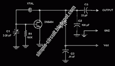
This circuit is a conventional Pierce-type oscillator that utilizes a JFET. It operates with fundamental mode crystals, offering decent performance and reliability when a low noise JFET is employed. The feedback is regulated by the capacitance of C1 from...
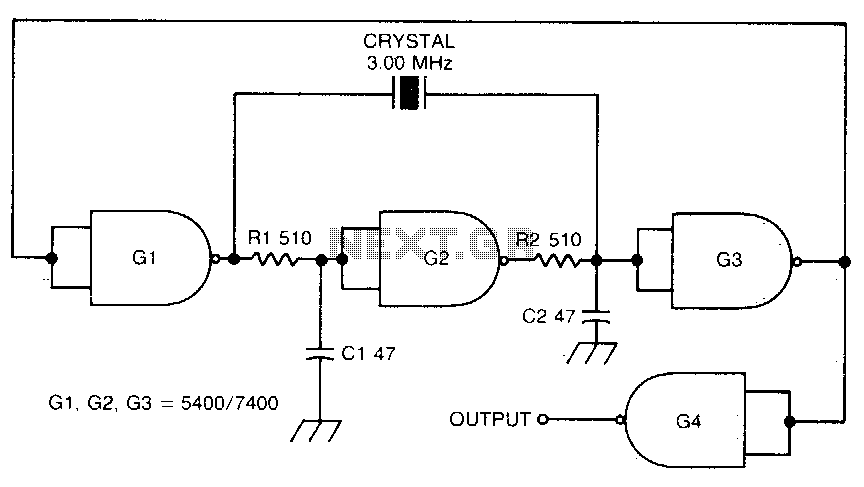
This circuit oscillates without the crystal. When the crystal is included in the circuit, the frequency will match that of the crystal. The circuit exhibits good starting characteristics even with low-quality crystals. This circuit design features a basic oscillator configuration...
The variations, which effectively form an alternating signal, will be transmitted through the coupling capacitor to the subsequent stage, indicated by the arrow to the right. One variable resistor can be substituted with another. R1 can be replaced with...