
Capacitance to voltage meter

The diagram indicates that when the value of Cx is small, the duty cycle is relatively low. The output pulses are narrow, resulting in a lower average DC voltage level at the output of U3. As the capacitance of Cx increases, the duty cycle rises, causing the output pulses from U2 to widen and the average DC output level at U3 to increase. The graph plots capacitance values from 0.01 µF to 0.1 µF against the output voltage of U3, demonstrating excellent linearity and a direct one-to-one scale calibration of the meter. If linearity issues arise, the 100 kΩ resistor, R1, can be replaced with a potentiometer to allow for adjustment to the appropriate value for the meter being utilized.
The circuit features a free-running oscillator, implemented with timer U1, which generates a consistent frequency of 60 Hz. This frequency serves as the basis for generating trigger pulses for timer U2. Timer U2, configured in monostable mode, produces output pulses whose width is determined by the capacitance of Cx. The relationship between Cx and the duty cycle is critical, as it influences the average DC output voltage from U3.
Resistor R1, a fixed resistor, is essential for establishing the circuit's timing characteristics. Capacitor Cx, the component under measurement, directly affects the output characteristics of the circuit. The output of U2 is fed into U3, which acts both as a low-pass filter and a unity-gain follower. This configuration ensures that high-frequency components of the output pulses are attenuated, allowing for a smooth DC voltage output that reflects the average value of the pulse train.
The output from U3 is expected to exhibit linearity with respect to the capacitance values being measured. The described graph demonstrates this linear relationship, providing a clear calibration scale for the circuit. Should the output not align with the expected values, the inclusion of a potentiometer in place of R1 allows for fine-tuning of the circuit, ensuring accurate measurements across the specified capacitance range. This adaptability enhances the circuit's utility in various measurement applications.Timer Ul operates as a free-running oscillator at 60 Hz, providing trigger pulses to timer U2 which operates in the monostable mode. Resistor Rl is fixed and capacitor Cx is the capacitor being measured. While the output of U2 is 60 Hz, the duty cycle depends on the value of Cx. U3 is a combination low-pass filter and unity-gain follower whose dc voltage output is the time-averaged amplitude of the output pulses of U2, as shown in the timing diagram.
The diagram shows when the value of Cx is small the duty cycle is relatively low. The output pulses are narrow and produce a lower average dc voltage level at the output of U3. As the capacitance value of Cx increases, the duty cycle increases making the output pulses at U2 wider and the average dc level output at U3 increases. The graph illustrates capacitance values of 0.01 ?Â¥ to 0.1 ?Â¥ plotted against the output voltage of U3.
Notice the excellent linearity and direct one-to-one scale calibration of the meter. If this does not occur the 100 k ohm resistor, Rl, can be replaced with a potentiometer which can be adjusted to the proper value for the meter being used.
Related Circuits
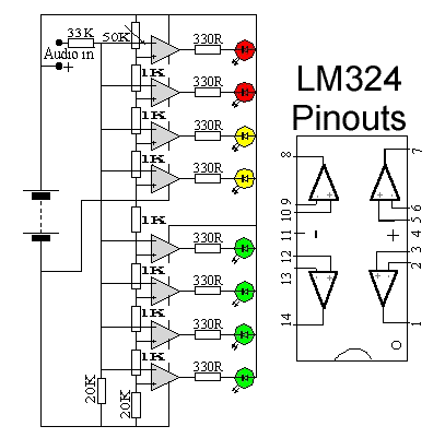
This circuit utilizes two quad op-amps to create an eight LED audio level meter. The op-amp employed in this circuit is the LM324, a widely used integrated circuit that is readily available from numerous electronic component suppliers. The 1K...
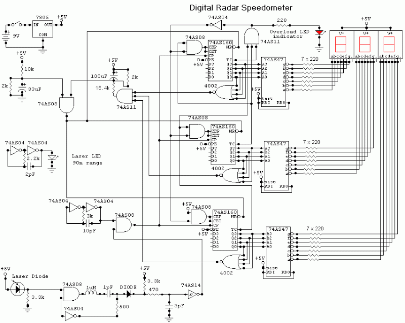
This digital alarm speedometer circuit allows for the measurement of the acceleration of any moving object, particularly cars and other vehicles. The acceleration is displayed in kilometers per hour (KPH) with a three-digit display. The system operates using laser...
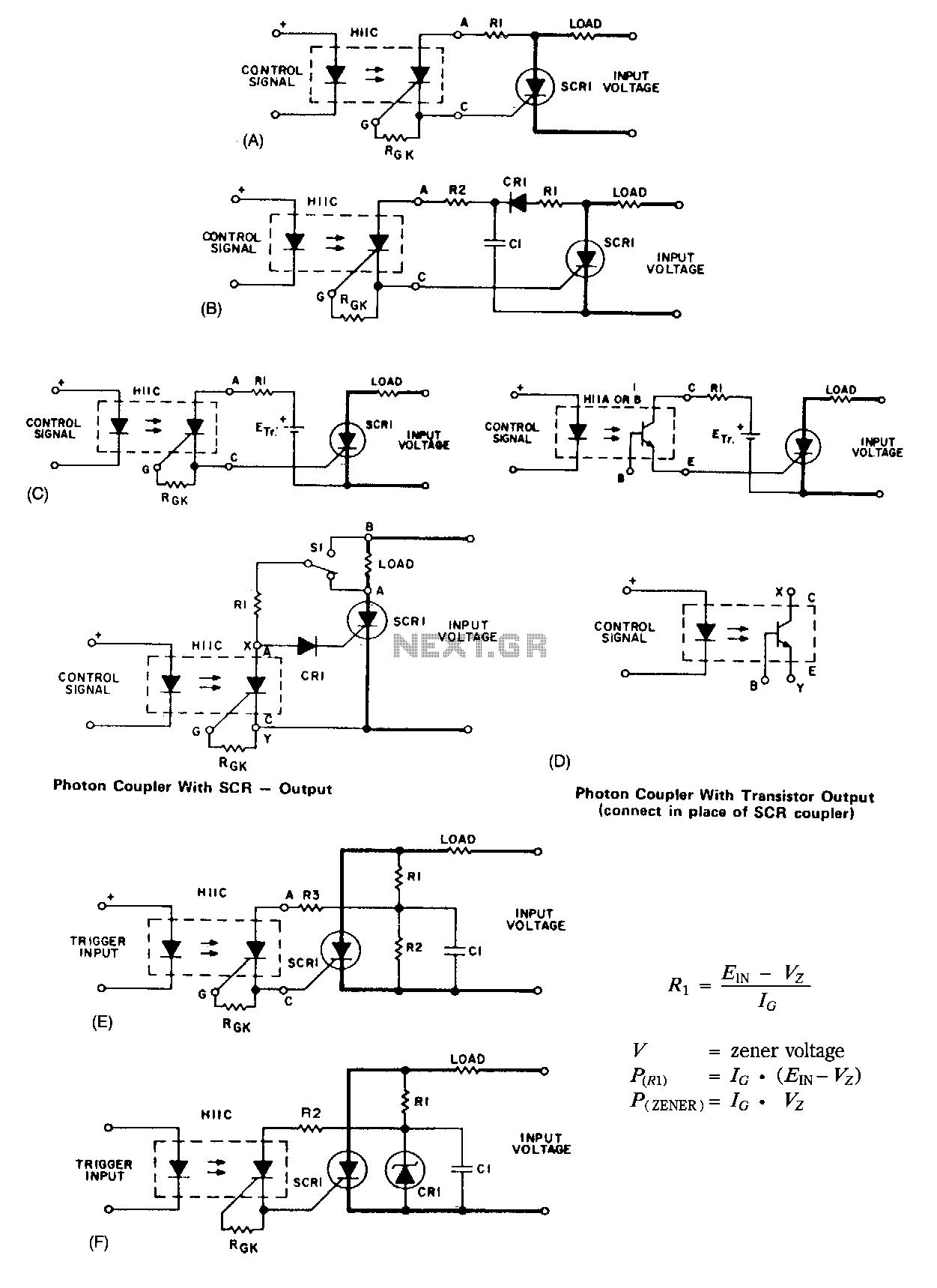
A basic circuit to trigger a silicon-controlled rectifier (SCR) is illustrated in Figure 67-1A. This circuit has the limitation that the blocking voltage of the photonic coupler output device dictates the circuit's blocking voltage, despite the SCR's higher voltage...

The inverting input is maintained at a low level via a 10K resistor when the circuit is powered on but not in use. During measurement activities, including calibration measurements where the input is floating, this resistor is disconnected. The...
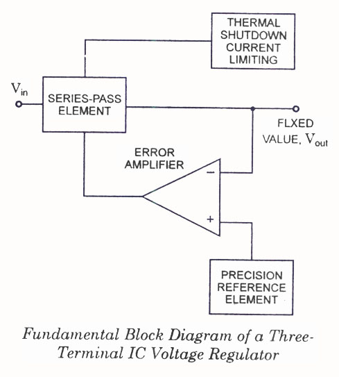
IC Voltage Regulators - Circuit diagram and block diagram of linear, fixed, adjustable (positive and negative), and switching voltage regulators. IC voltage regulators are essential components in electronic circuits, providing stable output voltages from a varying input voltage source. They...
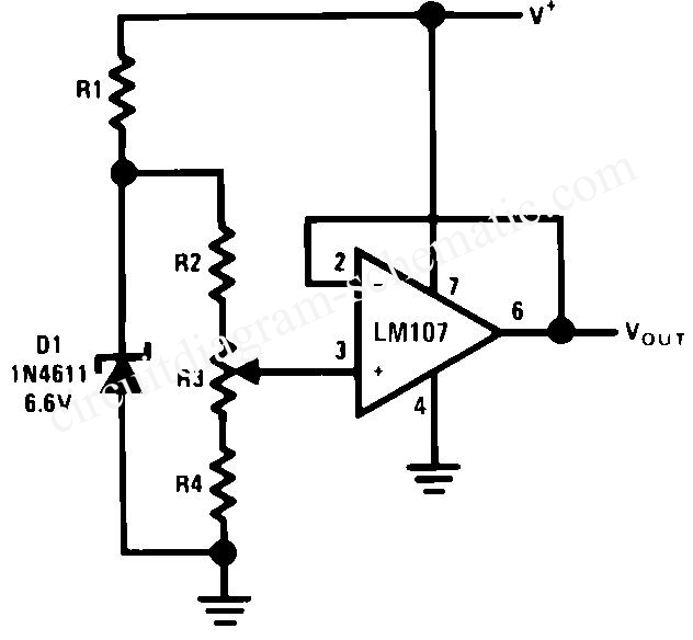
The circuit is designed for high precision operation over an extended temperature range, provided that V+ remains relatively constant, as the current IZ is dependent on V+. Resistors R1, R2, R3, and R4 are selected to ensure the appropriate...