
Capacitive load drive circuit diagram of the MAX4106 4107

The MAX4106 and MAX4107 operational amplifiers are designed for high-speed applications, featuring a wide bandwidth and low distortion. The inclusion of an isolation resistor (Rs) is crucial when interfacing with capacitive loads, as these loads can introduce instability in the feedback loop, leading to undesirable oscillations. The isolation resistor serves to dampen these oscillations by introducing a controlled amount of resistance, which increases the phase margin and enhances stability.
When selecting the value for Rs, it is important to consider the specific application and the characteristics of the load. A resistor value between 10 and 20 ohms is generally effective for most applications, but fine-tuning may be necessary based on the load's reactance. The interaction between the isolation resistor and the capacitive load can significantly influence the performance of the amplifier.
The MAX4106 is optimized for a gain of 5V/V with a feedback resistor (RF) of 120 ohms, while the MAX4107 is configured for a gain of 10V/V with a feedback resistor of 270 ohms. These gain settings allow for flexibility in various applications, enabling the user to achieve the desired output level while maintaining signal integrity. Careful consideration of the feedback network design is essential to ensure optimal performance, as it directly affects the bandwidth and stability of the amplifier circuit.
In summary, the MAX4106/4107 operational amplifiers, when used with an appropriate isolation resistor and feedback network, can effectively drive capacitive loads while minimizing the risk of overshoot and ringing, thus ensuring reliable performance in high-speed electronic applications. As shown in FIG grounds MAX4106/4107 using a capacitive load drive circuit isolation resistor Rs constituted. MAX4106/4107 good AC characteristics, but they are not designed to drive high reactive load, such as using a high reactive load will reduce the phase margin, causing a pulse signal overshoot ringing and ringing. The circuit can eliminate the above problems may arise between the output terminal and the load applied isolation resistor Rs, can be used to suppress overshoot and ringing oscillation, Rs is resistance of 10 ~ 20.
When the chip MAX4106, and RF when 120, a gain of 5V/V; when the chip MAX4107, and RF to 270 at a gain of 10V/V.
Related Circuits
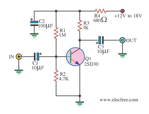
When there is a need to amplify audio signals from various sources before they reach a custom amplifier, a preamplifier (or preamp) is typically employed. This document suggests a specific circuit that is interesting due to its use of...
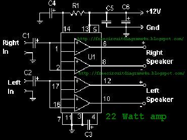
The function of the sound level display circuit is to enhance the appearance of an amplifier circuit or a radio player. It provides an impressive visual representation of audio levels. The sound level display circuit serves as a visual indicator...

All components used in the Moving Sensor/Detector Schematic Diagram utilize the IC NE555 and the Phototransistor L14F. The primary component in this circuit is the IC NE555, along with an IR LED, the Phototransistor L14F, and the IC LM1458....
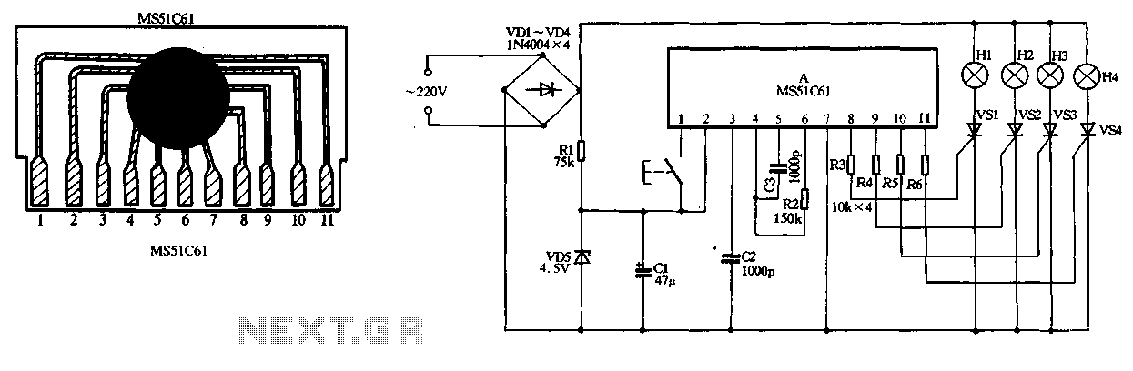
The circuit utilizes a 220V AC input, which is converted to DC using a VD1-VD4 bridge rectifier. This rectified voltage is used to power four lights (H1 to H4). The circuit also includes a resistor (R1) for voltage limiting...
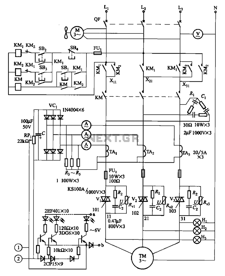
The circuit illustrated in Figure 3-178 is designed for controlling the speed and torque of a motor used in a continuous casting machine. It consists of the main circuit, a trigger circuit, and both manual and automatic control signal...

This project utilizes DTMF (dual-tone multi-frequency) signals, commonly used in telephones for dialing digits, as control codes. The DTMF tones are employed for frequency modulation of the carrier signal. At the receiver unit, these frequency-modulated signals are intercepted to...