
Capacitive load drive circuit diagram of the MAX4450 4451

The MAX4450 and MAX4451 are high-speed operational amplifiers designed for applications requiring precise signal integrity and fast response times. In this context, the use of a capacitive load drive circuit is essential for ensuring stable operation when driving capacitive loads, which can introduce unwanted feedback and oscillations.
The isolation resistor (RISO) plays a critical role in this configuration by providing a damping effect. By placing RISO in series with the output, it helps to reduce the amplitude of any overshoot that may occur when the output transitions rapidly. This is particularly important in high-frequency applications where the risk of ringing oscillations can lead to signal distortion and potential damage to the output stage of the amplifier.
The specified resistance range of 20 to 30 ohms is optimal for balancing the trade-off between signal integrity and stability. A lower resistance may not sufficiently dampen the oscillations, while a higher resistance could degrade the signal quality and increase the output voltage drop. Therefore, careful selection of RISO is essential to maintain the performance characteristics of the MAX4450/4451 in applications where capacitive loads are present.
In summary, the integration of an isolation resistor in the capacitive load drive circuit for the MAX4450/4451 enhances the stability and reliability of the amplifier's performance by effectively managing overshoot and ringing, ensuring high fidelity in signal transmission. As shown in FIG grounds MAX4450/4451 using a capacitive load drive circuit isolation resistor RISO constructed. The circuit between the output terminals and the load plus a res istor RISO, for suppressing overshoot and ringing oscillation, RISO resistance is 20 ~ 30 .
Related Circuits
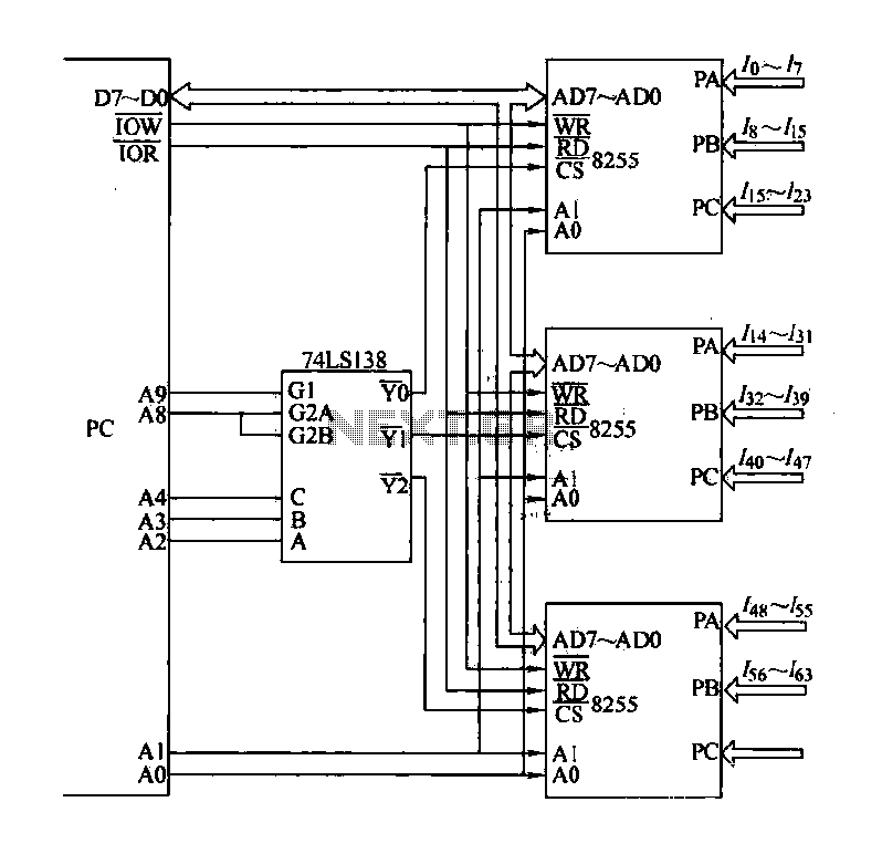
The computer control system is designed to detect signal path switching, requiring multiple input interface expansions. This system can switch all signal inputs into the computer. By utilizing a programmable chip, the 8255 expansion input interface allows for three...
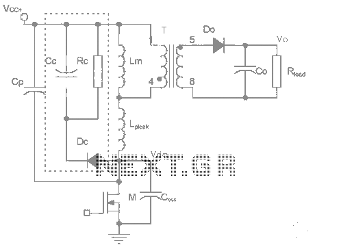
The work process analysis circuit diagram illustrates the use of a flyback converter transformer model. The flyback transformer primarily consists of ideal transformer magnetizing inductance and leakage inductance components. The flyback converter circuit exhibits high-frequency resonance at both ends...

Cable and xDSL modems are increasingly popular, leading to a need for designs that interface with existing telephones at subscriber locations. The subscriber line interface circuit (SLIC) within the modem must ring the phone and provide loop current during...
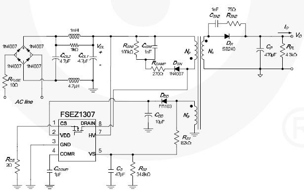
This cell phone charger circuit diagram electronic project is based on the FSEZ1307 third-generation primary side regulation (PSR) PWM controller integrated circuit. The FSEZ1307 cell phone charger can be used for battery charger applications for devices such as cellular...

Designing an audio amplifier from scratch using discrete components is an engaging task, as it enables users to create amplifiers that meet diverse requirements. Audio amplifiers can enhance low-level sounds from mobile devices, making them louder and more vibrant....
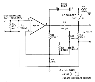
The circuit contributes 3.2 nV/√Hz of voltage noise and 0.45 pA/√Hz of current noise. To minimize noise from other sources, resistor R3 is configured to 100 ohms, resulting in an additional voltage noise of only 1.3 nV/√Hz. Resistors R1,...