
Flyback converter circuit Clamp

The flyback converter is a type of switched-mode power supply that utilizes a transformer to provide electrical isolation and voltage conversion. The core components of the flyback converter include the transformer, switch (typically a MOSFET), diode, capacitor, and load. The flyback transformer operates in two phases: during the switch's ON state, energy is stored in the transformer's magnetizing inductance; when the switch is turned OFF, the stored energy is transferred to the output through the leakage inductance.
In the circuit diagram, the switch is connected to the primary winding of the transformer. When the switch is closed, current flows through the primary winding, generating a magnetic field and storing energy in the transformer. The voltage across the switch increases due to the high-frequency operation, and the energy stored in the leakage inductance is released to the output capacitor when the switch opens. This process results in a voltage spike (VSPIKE) that adds to the output voltage, leading to a total output voltage of (VOR + VSPIKE).
The capacitor, which is connected to the secondary winding, plays a crucial role in smoothing the output voltage. The resistor in parallel with the capacitor helps to discharge the capacitor, ensuring that the voltage returns to its nominal value (VOR) before the next cycle begins. Proper design of the resistor and capacitor values, along with the selection of a suitable transformer, is essential to optimize the performance of the flyback converter, ensuring that energy is efficiently transferred and that voltage levels remain stable throughout the operation.
In summary, the flyback converter circuit is a sophisticated design that effectively manages energy transfer through careful manipulation of inductance and capacitance, ensuring reliable voltage output while minimizing losses and maximizing efficiency.In the work process analysis circuit diagram, for example, and use of work in flyback converter transformer model. Flyback transformer is mainly composed of ideal transformer magnetizing inductance and leakage inductance components. Figure flyback converter circuit Clamp Leaving the high-frequency resonance occurs at both ends of the switch DS voltage increases, but due to the leakage inductance energy can be generated VSPIKE timely transfer to the CC, leaving the terminal voltage CC rose from the secondary reflector to the maximum voltage VOR (VOR + VSPIKE); when the switch is turned on, CC through the resistor RC discharge tube so that the next cycle before the switch is turned off, the voltage can be made to recover from CC (VOR + VSPIKE) to the VOR. Thus, as long as a reasonable set of time constants, we can guarantee within one cycle will be transferred to CC leakage inductance energy release is completed.
Related Circuits
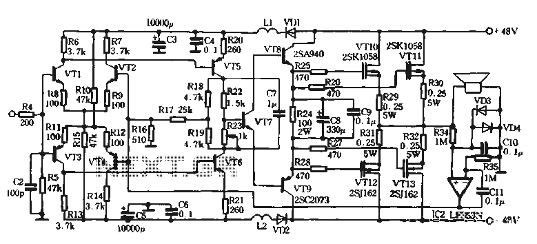
The self-designed amplifier circuit described is completely symmetrical and complementary, effectively utilizing the advantages of complementary NPN and PNP transistors to achieve a high degree of stability. The circuit features good symmetry in the push-pull amplification state, allowing for...

This is a 100-watt transistor inverter circuit diagram that features a straightforward design. The circuit utilizes only transistors, eliminating the need for integrated circuits. It converts a 12V battery input into a 220V output with a 50Hz square wave...
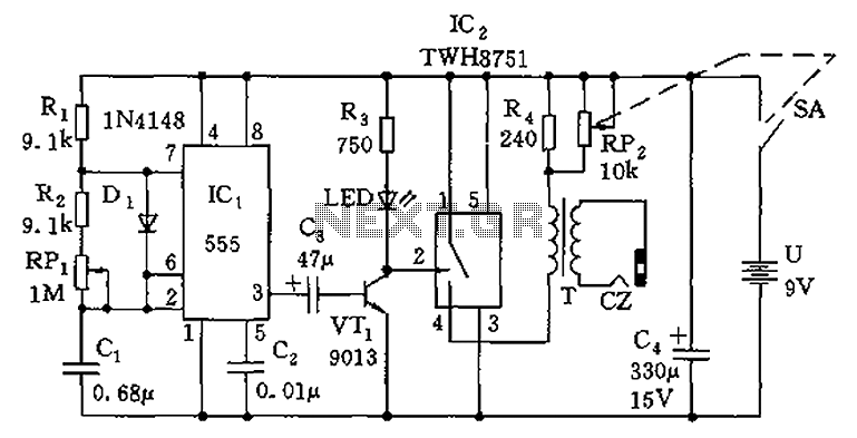
The circuit is composed of a 555 oscillator and an amplifier driver stage. It includes the 555 timer along with resistors R1, R2, RP1, capacitor C1, and other components forming a multi-harmonic oscillator. The frequency can be adjusted using...
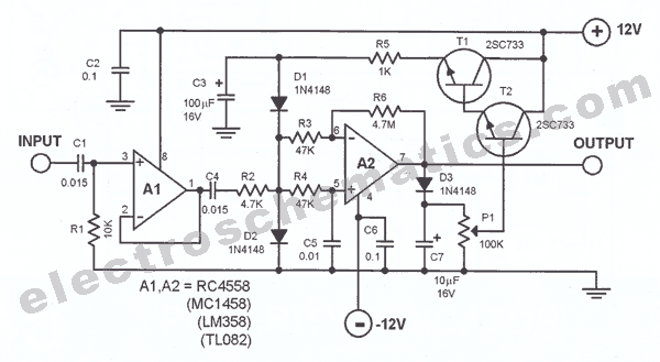
AVC - The circuit regulates the volume line automatically, providing an output voltage of approximately 4 volts peak to peak. This voltage remains consistent. The Automatic Volume Control (AVC) circuit is designed to manage audio levels dynamically, ensuring a stable...
This device is a combination digital clock timer and solar panel charge controller designed to maintain a deep cycle battery charged by a solar panel. The timer output controls a 12-volt load for a 32-minute interval each day. The...
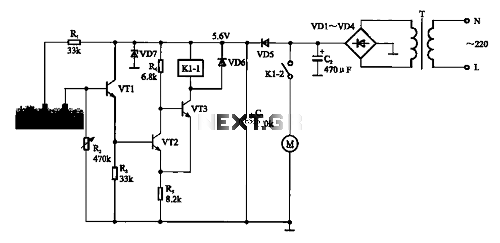
Automatic sprinkler control circuit. This circuit primarily consists of a humidity sensor, a detection signal amplifying circuit (including transistors VT1, VT2, and VT3), a power supply circuit (comprising a filter capacitor C2, a bridge conditioning circuit UR, and a...