
CF1 CF2 main circuit

The described circuit primarily functions as a power control mechanism for three-phase asynchronous motors using a single-phase AC supply. The initial AC voltage is rectified by a bridge rectifier composed of diodes VD1 to VD4, converting it into pulsating DC. Resistor R1 limits the current to ensure that the system operates within safe limits. Diode VD5 serves to clip any excessive voltage spikes, protecting the circuit from potential damage.
The trapezoidal wave generated in the circuit acts as a synchronization signal for the subsequent operation of the transistors. When a forward bias is applied to the base of VT1, it activates the transistor, allowing current to flow from the collector to the base of VT2. This setup enables VT2 to function as a variable resistor, allowing adjustments to the charging time constant of capacitor C3, which is crucial for timing control in the circuit.
As C3 charges, the voltage across it increases until it reaches a threshold where it can trigger VT3. The rapid increase in emitter current at VT3 leads to a quick discharge of C3 through R3, generating a sharp pulse output. This pulse, while initially small in amplitude, is amplified by VT4 to ensure it is sufficient to trigger the thyristor (VS1) for controlling the main load.
The use of a transformer in conjunction with VT4 allows for isolation and amplification of the pulse signal, ensuring reliable operation of the thyristor. The thyristor VS1, when triggered, controls the AC supply to the three-phase motors, allowing for efficient operation and control of motor speed and torque.
Capacitor C1 plays a critical role in phase shifting, which is essential for the operation of three-phase motors. The combination of resistive and capacitive elements in the circuit provides necessary protection and ensures stable operation under varying load conditions. The design also incorporates series resistance for additional protection, making the circuit robust against transient conditions.
Overall, this circuit exemplifies a well-structured approach to controlling AC motors using precise timing and synchronization techniques, enhancing the performance and reliability of industrial motor applications.AC voltage is rectified by a bridge (VD1-VD4). 3R1 limiting buck, VD5 clipping, a trapezoidal wave as the trigger circuit DC voltage and synchronization. When VT1 base of RP1 r eceived forward voltage is turned on, a collector coupled directly VTZ base, VT2 play a variable resistance action to change the 3cl capacitor charging time constant. When VT2 Yuetong, its collector to 3 cl charging, when charging voltage Uc Up (single-junction transistor peak voltage), VT3s e, resistance between bl sharp decline, while turned ON, the emitter current increase suddenly increase, 3G capacitive discharge by 3Ra, the VT3s bl have a sharp pulse output.
Since bl output pulse amplitude is too small, the VT4 amplification by Mr pulse transformer output - connected to the VS1 G and K, triggering VS1 conduction, when Ue
Related Circuits
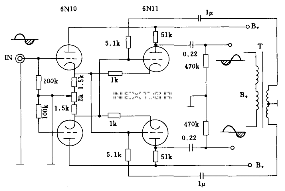
Balanced cross tube inverter circuit, also known as the Chelles inverter circuit, can be utilized as a preamplifier and employs 6N10 and 611 tubes in an inverted configuration. The circuit is designed to work with a final amplifier tube, specifically...
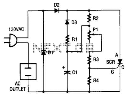
This circuit allows any standard household bulb to shimmer or blink. It is compatible with incandescent lights up to 200 W and operates on standard 120 Vac. The circuit employs a silicon-controlled rectifier (SCR) to create the shimmering effect....
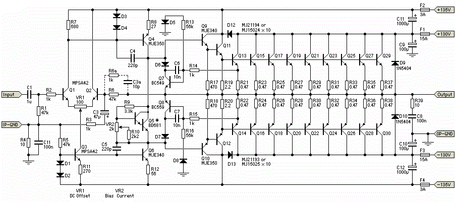
The circuit for the power amplifier has a power output of up to 1500W RMS and is commonly utilized in outdoor sound systems. The final image displays a series of power amplifiers that utilize 10 sets of power transistors....

Most of the power supply failure indicator circuits need a separate power supply for themselves. But the alarm circuit presented here needs no additional supply source. It employs an electrolytic capacitor to store adequate charge, to feed power to...
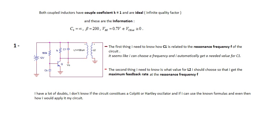
The first thing to understand is how capacitor C1 is related to the resonance frequency f of the circuit. It appears that selecting a frequency allows for the automatic determination of the necessary value for C1. There are uncertainties...

A compact audio amplifier circuit utilizing the TDA 7052 integrated circuit from Philips. This circuit is suitable for use as a pocket radio amplifier, delivering an output power of 2 watts. The TDA 7052 is a low-voltage audio amplifier designed...