
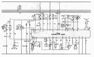
CF8865 module using dedicated switching power supply circuit diagram

The CF8865 switching power supply circuit is designed for high efficiency and reliability in power conversion applications. It operates at a frequency of 120kHz, which allows for smaller transformer and filter components, enhancing the overall compactness of the design. The excitation transformer Tz plays a critical role in controlling the operation of the output transistors VT4 and VTs, ensuring that they switch on and off appropriately to maintain the desired output voltage levels.
The circuit's feedback mechanism is crucial for maintaining voltage stability. The voltage sampling at pins 1 and 2 allows the CF8865 to monitor the mains input fluctuations and respond accordingly. This feedback loop ensures that any variations in the input voltage are compensated for by adjusting the pulse width modulation (PWM) at the output, thus maintaining a steady output voltage.
The use of a bridge rectifier following the pulse transformer ensures that the AC output is efficiently converted to DC. The voltage regulator then smooths the output, providing stable DC power supplies of 18V and 50V, which can be utilized for various electronic applications. The symmetrical nature of the output makes the circuit suitable for powering devices that require dual voltage supplies.
In summary, the CF8865 switching power supply circuit is a sophisticated design that combines advanced control mechanisms with efficient power conversion techniques. Its ability to adapt to input voltage fluctuations while providing stable output voltages makes it an ideal choice for modern electronic systems that demand reliability and performance.Described here is a specific module using CF8865 switching power supply circuit, because this circuit is the use of integrated control module CF8865 specific modules. In the fi gure, VT4, VTs is controlled by the excitation transformer Tz job switch, its output down by a pulse transformer T3, followed by stage output voltage bridge rectifier and regulator, the filtered output of plus or minus two symmetrical DC power supply, which is a group of 18V, another group of 50V. CF8865 can produce oscillation pulse 120kHz from 3,4 pin output module through the excitation transformer T and push the switch VT4, VTs work.
CF8865 9-pin output voltage adjustment ends, RPi to adjust potentiometer, adjust Wei, you can change the output voltage value of 08 feet for the output voltage error sample input voltage. l, 2 feet for the mains input voltage fluctuation sampling control input, since CF8865 3.4 foot addition to the excitation pulse to promote the output transformer Tz VT4, VTs turned off, but also to promote the vrl turned off by another winding.
When the mains voltage fluctuations, 300V DC voltage rectifier output will fluctuate, so that by the VTi is turned off amplitude pulses across the primary winding Ti formed will fluctuate after it is coupled to the secondary station via VD4 rectifying generated negative voltage amplitude will be crossing the move, and the potential difference between the change in 2,1 feet, after an internal NIE circuit detection to control the output of 3,4 feet pushing pulse width, and ultimately mains fluctuations caused by fluctuations in the output voltage will be regulated to control.
Related Circuits
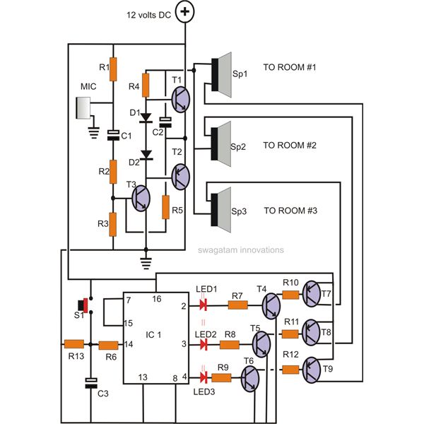
A home intercom system can be constructed using a versatile circuit design. This system allows communication across up to ten different locations or rooms discreetly. It utilizes a single changeover switch for selecting the desired location, replacing the traditional...

The circuit is designed for teaching demonstrations or experiments to hear the electrocardiogram (ECG) signal voltage. The ECG signal voltage is amplified by the LM4250 operational amplifier, which is connected to a voltage-controlled oscillator (NE566) to modulate the oscillator...
The following document contains information related to the electrical installation schematic diagram for the Volvo 440. It includes the wiring schematic for the Volvo 440, 460, and 480 series. The Volvo 440, 460, and 480 series vehicles feature a comprehensive...
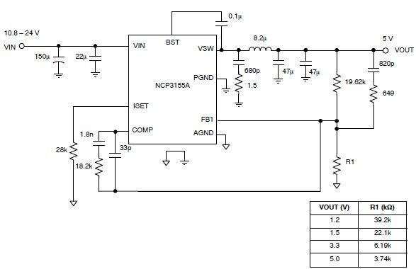
This 5-volt regulated power supply circuit project is designed using the NCP3155 DC-DC switching regulator, which features fully integrated power switches and comprehensive fault protection. The circuit requires only a few external electronic components and delivers a fixed output...

The schematic presented is a project for a simple temperature sensor circuit, also referred to as a heat sensor circuit, which activates an LED in response to heat. The circuit is straightforward to construct and requires only a few...

A simple dimmer circuit can be constructed using the CMOS ICs TT8486A and TT6061A, allowing control over the intensity of an incandescent lamp through a touch contact. This electronic touch dimmer can increase the brightness of incandescent lamps in...