
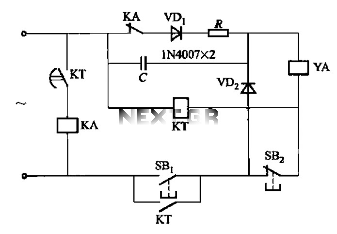
Charging time relay circuit 2

The charging time relay circuit operates by utilizing a large capacitor (C) rated at 5000 µF, which is responsible for providing a long delay period of up to 1.3 hours. The circuit employs two main transistors, VT1 and a pair of voltage regulators, VS2 and VS3, configured to function as a constant current source. This configuration enhances the precision of the delay time, ensuring that the circuit performs reliably under varying conditions.
When the user presses the switch (SB), the relay (KA) is activated, which leads to the deactivation of transistor VT2 and the activation of transistor VT3. This initial state allows the circuit to begin its timing function. After the predetermined delay period, controlled by the charging of the capacitor, transistor VT2 is turned on, which subsequently turns off VT3, resulting in the release of relay KA.
The delay time can be finely adjusted using the potentiometer (RP), providing flexibility in applications where different timing intervals are required. The design of this circuit is ideal for applications where a precise delay is necessary, such as in timing circuits, automated systems, and control applications. The combination of the large capacitor, constant current source, and adjustable potentiometer ensures accurate and customizable delay timing, making this relay circuit a valuable component in various electronic systems. Charging time relay circuit 2 It is a long delay circuit. When the capacitor C is 5000yF, the delay can be up to 1. 3h. By transistors VTi and regulator VS2, VS3 group as a con stant current source, in order to improve the accuracy of the delay. Press the button SB, KA relay pull, VTz off, VT3 conduction. After after a delay, VTz conduction, VT3 deadline, KA released. Adjustment potentiometer RP, adjust the delay time.
Related Circuits
The Zener diode may not be providing sufficient current in its breakdown state to activate the transistor. Removing resistor R2 did not resolve the issue. The Zener's voltage selection could be too high, potentially preventing it from regulating the...
AC solenoid DC circuit operation operates similarly to a DC contactor circuit, but the AC solenoid pull circuit is illustrated in the provided figure. The capacitance C is generally between 1-10 microfarads (µF), with a minimum of 20 microfarads...

This operational amplifier circuit utilizes resistor and transistor feedback elements to function as a nonlinear amplifier. The resistors R4 and R6 can be adjusted to modify the breakpoints as needed. This operational amplifier circuit is designed to operate within the...

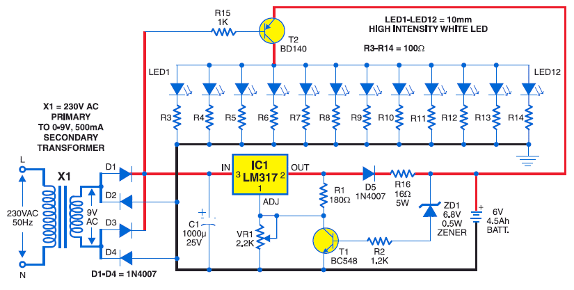
This colorful backlit aquarium light provides a natural appearance to the aquarium tank. The aquarium LED lighting circuit automatically turns on at sunset. The aquarium LED lighting system enhances the aesthetic appeal of the aquarium by simulating natural lighting conditions....
Uploaded with ImageShack.us Uploaded with ImageShack.us Uploaded with ImageShack.us Inquiry regarding experiences with specific circuits. In this context, the inquiry pertains to the performance and functionality of certain electronic circuits that have been shared via an image hosting service. The...
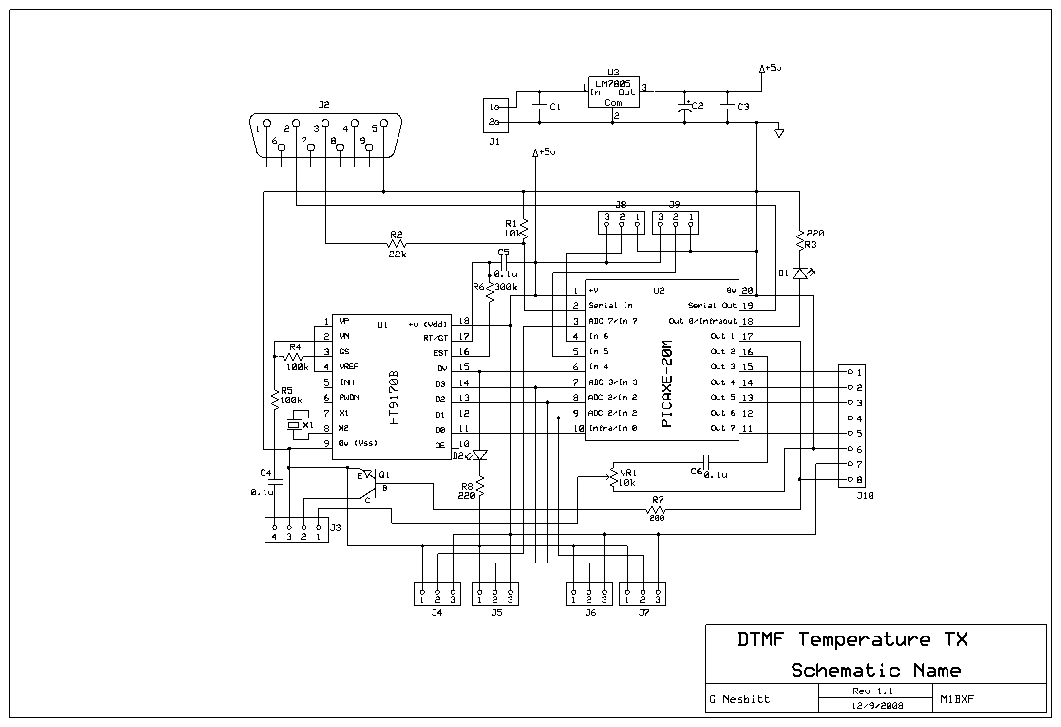
Remotely check the temperature of various items, specifically the repeater site at GB3PY. This system utilizes a radio to receive requests for the current temperature and sends the results back to the user. Requests are made using DTMF tones,...