
Circuit explanation of PLL synthesizing oscillator

The described circuit employs a phase-locked loop (PLL) architecture to achieve precise frequency control. The PLL synthesizer generates a stable output frequency that is critical for applications such as amateur radio transmission. By fixing the division ratio at 1024, the circuit ensures that the output frequency remains within the designated amateur radio bandwidth, effectively allowing for frequency agility within the specified range.
The variable capacitance diodes, D1 and D2, play a crucial role in tuning the VCO. These diodes are particularly sensitive to voltage variations, which makes them ideal for frequency modulation applications. As the reverse voltage applied to these diodes increases, the capacitance decreases, resulting in a shift in the oscillation frequency of the VCO. This tuning capability is essential for maintaining signal integrity and stability during operation.
The charge pump integrated into the MC145163 generates a pulse signal that is instrumental in controlling the VCO. This pulse signal is filtered through a network consisting of resistors R4, R5, R6, and capacitor C6, which smooths the output to produce a stable DC voltage. This voltage directly influences the VCO's oscillation frequency, allowing for fine-tuning of the output signal.
Furthermore, the inclusion of the FET in the circuit enhances the overall functionality by providing a means to control the drain current. The gate voltage applied to the FET determines the conductivity of the channel, thereby enabling control over the output current delivered by the VCO. This feature is particularly beneficial in applications requiring dynamic adjustments to the output signal, ensuring that the circuit can adapt to varying operational conditions.
In summary, this PLL-based circuit is designed for precise frequency control within the amateur radio spectrum, utilizing a combination of varicap diodes, a charge pump, and a field-effect transistor to achieve stable and adjustable oscillation frequencies.To change the frequency of the output by the dividing ratio of the comparison frequency in the 10KHz unit, the dividing ratio is fixing on 1024 at the circuit this time. Because the 144-MHz bandwidth of the amateur radio is 2MHz(144. 0MHz to 146. 0MHz) in Japan, it makes the output frequency of the PLL 133. 3MHz to 135. 3MHz. (Frequency with the low o f 10. 7MHz) The oscillation frequency of the voltage controlled oscillator is controlled by the output of the PLL synthesizer and does the oscillation operation of the stable frequency. D1 and D2 are the variable capacitance diode (the varicap diode). The capacitance of the diode changes when gaining opposite direction voltage. The capacitance becomes small when making opposite direction voltage high. The signal for the control which is output from the charge pump of MC145163 is a pulse signal. A pulse signal is changed into the voltage change of the direct current through the filter by R4, R5, R6 and C6.
The FET is an electric Field Effect-type Transistor. The output current (the drain electric current) can be controlled at the voltage which is gained by the input (the gate). 🔗 External reference
Related Circuits
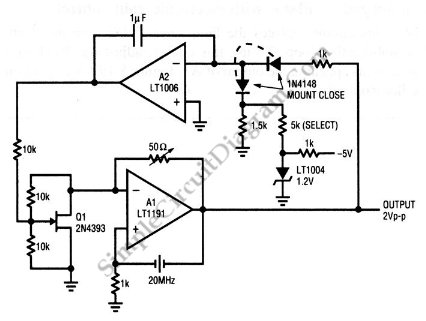
This is a quartz-stabilized oscillator circuit with electronic gain control. Replacing the common filament lamp for amplitude stabilization, this circuit uses... This circuit represents a quartz-stabilized oscillator featuring electronic gain control, which enhances the stability and precision of the output...
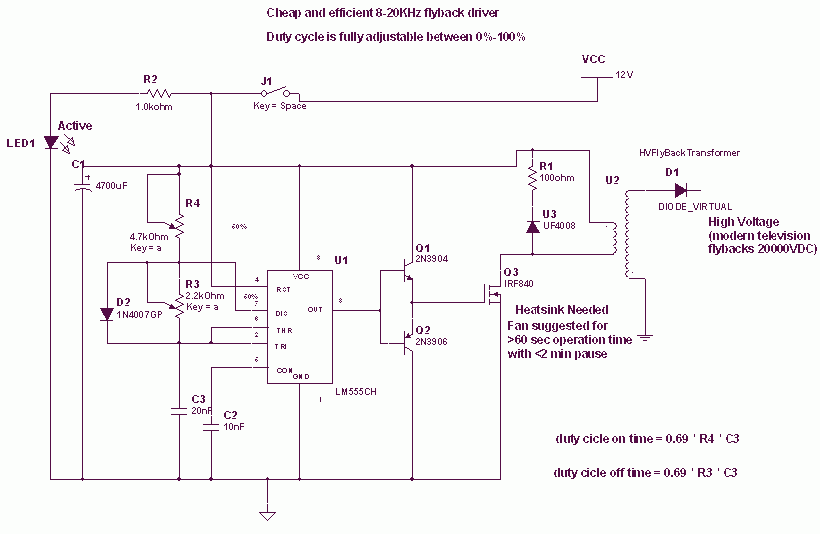
The 555 is wired as an astable and the capacitor is charged only through the 4.7Kohm trimmer (notice the diode) and discharged only through the 2.2 Kohm trimmer, making the duty cycle fully adjustable. The square wave is then...

This is a sensor circuit designed for light detection. It utilizes the LM311 comparator and features a simple design. The comparator is powered by a 12 V DC supply and does not require a negative supply for efficient operation....
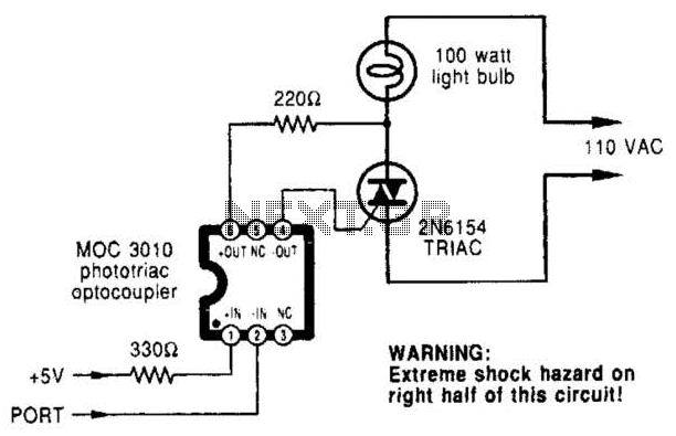
A microcomputer-to-triac interface utilizes a phototriac optoisolator to safely isolate logic signals, allowing direct control of high-power loads. This circuit can function as either an on/off switch or a proportional phase control, depending on the input waveforms and the...
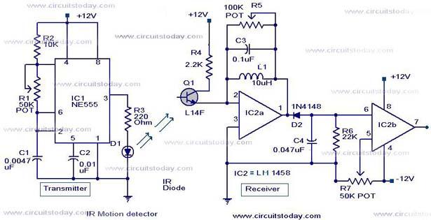
Infrared (IR) Motion Detector Circuit featuring a motion detector alarm and an infrared sensor. The circuit diagram and its operation are provided in detail. The infrared (IR) motion detector circuit is designed to detect motion within a specified range and...
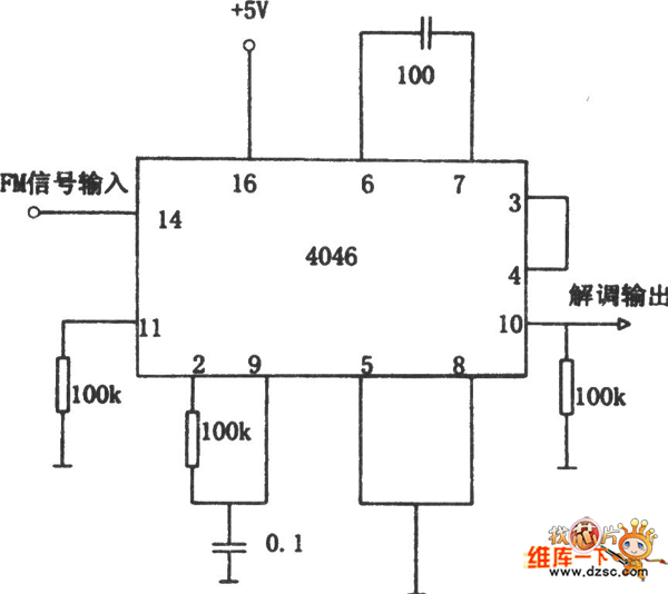
The FM demodulator circuit, as illustrated in the figure, utilizes a 4046 Phase-Locked Loop (PLL) integrated circuit to convert the intermediate frequency FM input signal into a lower frequency output. The FM demodulator circuit based on the 4046 PLL IC...