
Binary Up Counter Circuit with working animation and simulation video
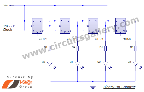
The Asynchronous 4-Bit Binary Up Counter operates by utilizing four J-K flip-flops, where each flip-flop represents one bit of the counter. The J-K flip-flop is a versatile digital memory circuit that can toggle its output based on the input conditions. In this configuration, the flip-flops are connected in such a way that the output of one flip-flop serves as the clock input for the next flip-flop in the sequence, creating an asynchronous behavior.
When the counter is activated, the least significant bit (LSB) flip-flop toggles its state with each clock pulse. This toggling occurs at a frequency determined by the clock signal fed into the first flip-flop. Each subsequent flip-flop toggles its state on the falling edge of the previous flip-flop's output, effectively dividing the frequency by two for each additional flip-flop. As a result, the counter counts in binary from 0000 to 1111 (0 to 15 in decimal).
In designing the circuit, careful attention must be given to the setup and hold times of the J-K flip-flops to ensure reliable operation. The circuit can be powered by a standard DC supply, and it is important to include debounce circuitry if mechanical switches are used to initiate the clock pulses.
Simulation tools can be employed to visualize the counting sequence and verify the operation of the counter. The accompanying video provides a practical demonstration of the circuit assembly, illustrating how to connect the components and observe the output states as the counter progresses through its counting sequence.
Overall, the Asynchronous 4-Bit Binary Up Counter is a fundamental digital circuit that serves as a building block for more complex counting applications in digital electronics. Its ease of implementation and straightforward design make it an excellent choice for educational purposes and practical applications alike.Here we are going to discuss about an Asynchronous 4 Bit Binary Up Counter, a circuit made up of several J-K flip-flops cascaded to generate four bits counting sequence. An up counter is basically a digital counting circuit which counts up in an incremental mode. Here we have given the simple counting circuit setup using 4 flip flops and a simulat ion video for better understanding. For simplicity, an animation outputofelectronic counter sequence is also provided with this article. After reading this article you will be able design Up Counter circuits easily. Watch this video of Binary Up Counter circuit simulation. In this video we have showed the step by step circuit assembly and output working of Digital 4 bit up counter circuit. You can also visit out Video Gallery for other videos. 🔗 External reference
Related Circuits
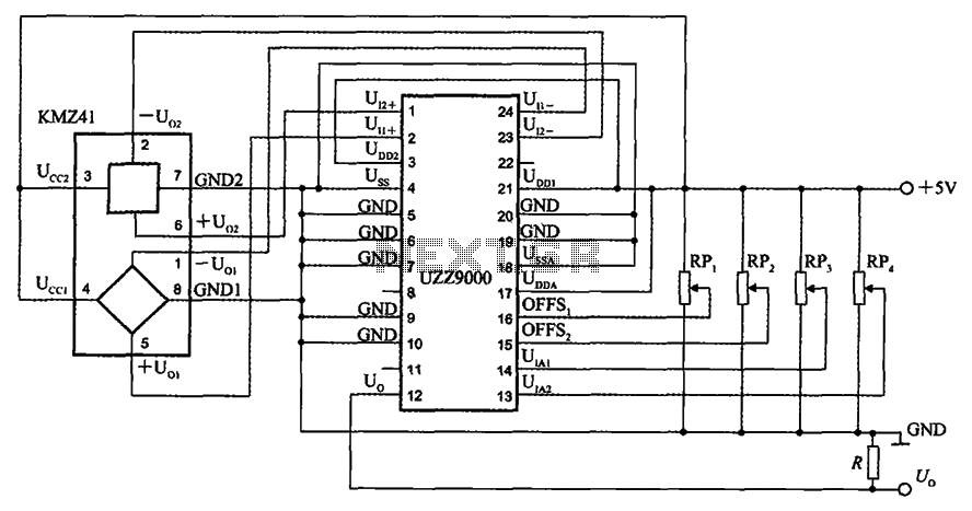
The UZZ9000 KMZ41 detection circuit is configured based on the voltage output type and angle. It operates with a +5V power supply. Potentiometers RP1 and RP2 are used for offset voltage adjustment, while potentiometers RP3 and RP4 are utilized...
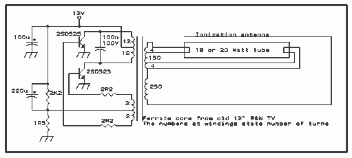
Here is the schematic diagram for a 20 Watt driver. I developed this circuit in 1985, and used it to build a lamp that found much use both as camping light and as emergency light during the then-frequent power...
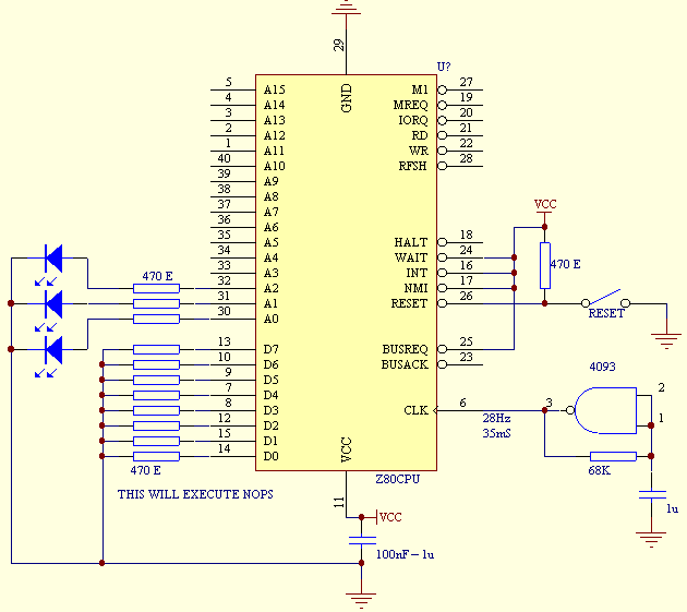
GND and VCC are positioned perpendicularly to the other pins in the circuit diagrams, while the actual Z80 is a DIP with no pins in these locations. This arrangement complicates the readability of the circuit diagram, necessitating a mapping...

The ADP3000 is an integrated circuit featuring a block diagram that illustrates its internal structure as a high-frequency switching regulator. The ADP3000 integrated circuit is designed to provide efficient power management in various applications, particularly in systems requiring high-frequency switching...
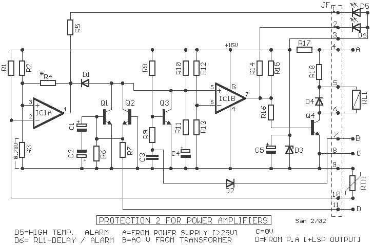
The protection circuit output amplifiers and speakers has some interesting features such as isolating the speaker from the amplifier output when shown a continuous trend in output or when the temperature gets too much cooler while providing a time...
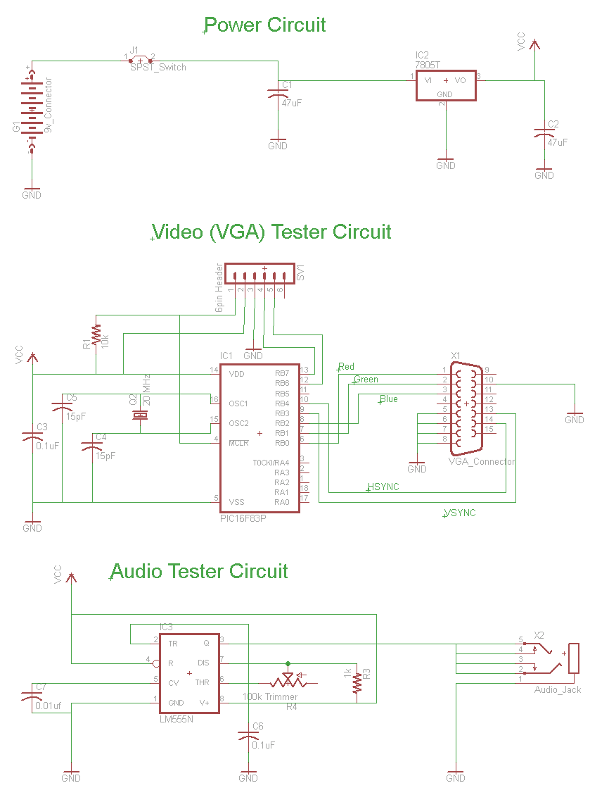
The Mini AV Test Box circuit is designed with simplicity and efficiency in mind. It consists of three main sections, which are clearly delineated in the schematic. The primary components utilized in this circuit include the 7805 voltage regulator,...