
Flash memory interface tutorial covering basic fundamentals
Flash memory is a critical component in modern electronic devices, providing a reliable and efficient means of data storage. Its non-volatile nature ensures that data remains intact even when power is lost, making it ideal for applications where data integrity is paramount. The architecture of flash memory cells, utilizing floating-gate MOSFET technology, allows for high-density storage solutions while maintaining performance standards.
In terms of applications, NOR Flash is particularly advantageous in scenarios where code needs to be executed directly from the memory, such as in embedded systems and firmware storage. Its random access capability allows for quick retrieval of data, which is essential for real-time applications. Conversely, NAND Flash excels in environments where large volumes of data are stored, such as in consumer electronics, digital cameras, and mobile devices. Its higher endurance and lower cost per bit make it the preferred choice for high-capacity storage solutions.
The evolution of flash memory has also led to advancements in data transfer speeds and storage capacity. The introduction of multi-level cell (MLC) technology has enabled manufacturers to increase storage density without significantly increasing the physical size of the memory chips. This innovation has facilitated the development of compact storage devices, such as USB drives and memory cards, which are widely used in various consumer electronics.
In conclusion, flash memory represents a significant advancement in data storage technology, combining speed, reliability, and efficiency. Its diverse applications and ongoing technological improvements continue to shape the landscape of electronic devices, driving innovation and enhancing user experiences across multiple sectors.Flash memory or a flash RAM is a type of nonvolatile semiconductor memory device where stored data exists even when memory device is not electrically powered. It`s an improved version of electrically erasable programmable read-only memory (EEPROM). The difference between Flash Memory and EEPROM are, EEPROM erases and rewrite its content one byte a t a time or in other words, at byte level. Where as Flash memory erases or writes its data in entire blocks, which makes it a very fast memory compared to EEPROM. Flash memory can`t replace DRAM and SRAM because the speed at which the DRAM/SRAM can access data and also their ability to address at byte level can`t be matched by Flash.
The flash memory is also termed as Solid-state Storage Device (SSD) due to the absence of moving parts in comparison to traditional computer hard disk drive. The two main types of flash memory are the NOR Flash & NAND Flash. Intel is the first company to introduce commercial (NOR type) flash chip in 1988 and Toshiba released world`s first NAND-flash in 1989.
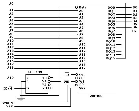
NOR-flash is slower in erase-operation and write-operation compared to NAND-flash. That means the NAND-flash has faster erase and write times. More over NAND has smaller erase units. So fewer erases are needed. NOR-flash can read data slightly faster than NAND. NOR offers complete address and data buses to randomly access any of its memory location (addressable to every byte). This makes it a suitable replacement for older ROM BIOS/firmware chips, which rarely needs to be updated.
Its endurance is 10, 000 to 1, 000, 000 erase cycles. NOR is highly suitable for storing code in embedded systems. Most of the today`s microcontrollers comes with built in flash memory. NAND-flash occupies smaller chip area per cell. This maker NAND available in greater storage densities and at lower costs per bit than NOR-flash. It also has up to ten times the endurance of NOR-flash. NAND is more fit as storage media for large files including video and audio. The USB thumb drives, SD cards and MMC cards are of NAND type. NAND-flash does not provide a random-access external address bus so the data must be read on a block-wise basis (also known as page access), where each block holds hundreds to thousands of bits, resembling to a kind of sequential data access. This is one of the main reasons why the NAND-flash is unsuitable to replace the ROM, because most of the microprocessors and microcontrollers require byte-level random access.
A write operation in any type of flash device can only be performed on an empty or erased unit. So in most cases write operation must be preceded by an erase operation. The erase operation is fairly straightforward in the case of NAND-flash devices. But for a NOR-flash, it is mandatory that all bytes in the target block should be written with zeros before they can be erased. The size of an erase-block in NOR-flash ranges from 64 to 128 Kbytes. Here a write/erase operation can take up to 5 s. But the NAND-flash has erase blocks 8 to 32 Kbytes in size. So it is obvious that the NAND performs the identical operation in a lesser time duration. INOR-flash interface resembles closely to a SRAM memory interface, which has enough address pins to map its entire media, allowing for easy access to every byte contained in it, where as the NAND-flash go for serially accessed complicated I/O mapped interface.
Here the same pins are used for control, address & data. In traditional single-level cell flash devices, each cell stores only one bit of information. Later, many developers have developed a new form of flash memory known as multi-level cell flash that can store/hold more than one bits rather than a single bit in each memory cell, thus doubling the capacity of memory. Flash memory stores data in an array of memory cells. The memory cells are made from floating-gate MOSFETS (known as FGMOS). These FG MOSFETs (or FGMOS in short) have the abilit 🔗 External reference
Related Circuits

Investigating a Paradox: Recently, an energy-saving LED flashlight was observed for sale that utilized only one 1.5-volt battery. Upon purchasing this light and disassembling it, the expectation was to find a battery, bulb, switch, and a circuit board designed...
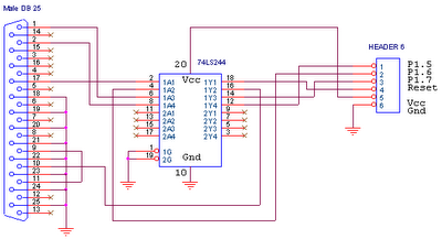
This circuit is designed for use with ATMEL Microcontroller ICs, specifically the AT89Sxx and ATMEGA series. It operates using the MISO, MOSI, SCK, and RESET signals. This circuit serves as a foundational interface for programming and communication with ATMEL microcontrollers,...
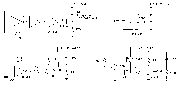
The LED flasher circuits below operate on a single 1.5 volt battery. The circuit on the upper right uses the popular LM3909 LED flasher IC and requires only a timing capacitor and LED. The top left circuit, designed by...
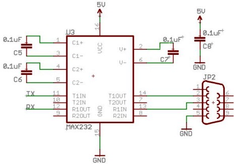
The UART, or Universal Asynchronous Receiver/Transmitter, is a feature of microcontrollers that facilitates serial data communication (text, numbers, etc.) with a PC. This device converts incoming parallel data (within the microcontroller/PC) to serial data that can be transmitted over...

Inverters IC1-a and IC1-b form a multivibrator, while IC1-c acts as a buffer. Inverter IC1-d is configured such that its output is the inverse of IC1-c; when pin 6 is high, pin 8 is low, and vice versa. As...
The ATA5423, ATA5425, ATA5428, and ATA5429 are highly integrated UHF ASK/FSK multi-channel half-duplex transceivers characterized by low power consumption. These devices are housed in a compact 7 x 7 mm QFN48 package. The receiving section features a fully integrated...