
PARALLEL BUS REVEALED Conclusion of the first-ever PBI usage guide
.jpg "PARALLEL BUS REVEALED Conclusion of the first-ever PBI usage guide")
All this assumes that we`re decoding addresses and that we have some software in ROM, so let`s get on with those details. The output signal $D8XX-$DFXX, combined with the Device Select signal (DEVSEL), provides the Math Pack Disable signal (MPD) to disable the floating point ROM in the CPU so it doesn`t contend with our ROM for the data bus.
We can use the same signal to select our ROM. This allows us to remove some of the logic from last month`s circuit. Just remove the wires from 1C4 pins 6, 5, 4, 13, 12 and 11 and connect MPD to ROM pin 20. (See last month`s Figure 2). The signal $DlFF selects the Device Enable Latch. When a write signal clocks the 74HCT74 latch, the value of the Data 0 line (D0) will be stored. Writing 1 to address $DlFF selects our external device. Writing 0 deselects it. $DlFF can also be used later to select an interrupt register. By combining it with DEVSEL and $DlXX, we get a Device Register Enable signal (DRE). We`ll use this signal instead of part of the logic in last month`s circuit to make the device registers work. Just remove the wires from 1C4 pins 3, 2 and 1, and connect DRST to 1C5 pin 13. The CPU External Enable signal (EXTENB) lets our device know the computer wants to talk to device registers (or RAM in a more complex application).
That signal is combined with DEVSEL and $DlXX to make an External Select signal (EXTSEL) to turn off CPU RAM so as to avoid bus contention. You`ve probably noticed that this month`s schematics are a little different from last month`s. Since last month`s circuit is the basic recipe for our device, we included IC location assignments and pin numbers.
This month`s article deals with several options you might or might not use, so we`re giving you IC type numbers and no pin assignments for general logic functions. The number inside or next to a symbol is its type number. For example, 00 means 74HCT00. Since all the logic is 74HCT series, we just need to use the last digits of the type number to identify a part.
Also, be aware that we use both positive and negative names for some signals. R/W and R/W are complementary signals and mixing them up won`t work. It would be nice to have a status register. That way, we could tell the state of our USART by asking it, rather than just hoping the byte we gave it got sent, or assuming the byte we got from it is a good one. The USART does have a status word available: four bits to read and a reset bit to write to. The read bits are three error bits: Over-Run (OR), Framing Error (FE) and Parity Error (PE), and a Transmit Buffer Empty bit (TBE).
The write bit is a Reset Data Available bit (RDAV). Last month`s signal name list explains these bits`s functions. In order to use this new register, we need to expand our addressing capability. Figure 2 shows a way to use the Address 0 line to select even and odd addresses in the device register space. Figure 3 shows an implementation of the status register. The 74HCT244 shown is a tri-state buffer. This allows us to read the status bits when we select any odd address in the device register space. The gate to the USART RDAV pin resets the Data Available flip-flop when we write anything to an odd address.
The IRQ line is there in case you want to design in an Interrupt Register. We`re assuming that we want to generate an interrupt when we get a Data Available signal from the USART. Figure 4 uses a 74HCT244 to make an interrupt register. This allows the OS interrupt handler to poll our Parallel Bus device to see who made an interrupt request.
By putting the IRQ signal on the Data 0 line, we have established our USART device as Device 0. Putting the signal on the Data 1 line would make it Device 1, Data 3 makes it Device 3, etc. Whatever bit you use here must correspond to the bit you use for the Enable Latch (Figure 1). The remaining bits must be tied to 0 (Ground). Remember that we`ve designed this circuit to be the only external device on the parallel bus. If you were to put several devices on the bus, things would get much more complex. Designing a multiple board system is beyond the scope of this article. But if you`re a serious hardware hacker, you can probably extend what we`ve done here for more than one function. You should also realize that the logic in this design can be streamlined in several places. We aimed for use of only a few IC types, and haven`t always optimized for speed or elegance. Sometimes we do things like use a NOR and an inverter to make an OR gate. Bulky, but workable. Now for software The only really awkward thing here is that you`ve got to have access to an EPROM programmer for 2716`s.
I used a cranky home-built programmer a friend put together. Most large users` groups have at least one member with access to one, so you might try there. The important part of the ROM is the vector table. You can put all your device driver routines on disk and load them as an AUTORUN. SYS file if you want, but the vector table MUST be in ROM. You can also put your device drivers in ROM if you want. For our example, we are only implementing INIT, PUT, GET, and STATUS. For simplicity, we`re making the drivers contiguous with the ROM vector table to run entirely from ROM. The drivers in Listing 1 were written using MAC/65 (Optimized Systems Software). The source code will also assemble using the Atari Assembler Editor cartridge. The drivers are thoroughly commented so it should be easy for you to see how they work. Notice that we reset the CRITIC flag at the beginning of each driver routine. The Generic Handler sets it in advance in case a parallel device is extremely time critical. Forgetting to reset CRITIC defeats some OS functions such as software counter timers and key repeat among others.
The rest of the code is very straightforward. Many thanks to Dave Menconi, formerly of Atari, for the easy-to-follow listing. Using these basic ideas with some ingenuity, you should be able to design your own parallel devices for your 800XL or 600XL computer. If you dream up an interesting project, the editors at Antic would like to hear about it. 🔗 External reference
Related Circuits

While conducting background research on the Philips I2C bus, an application note authored by Herman Schutte from Philips Semiconductors Systems Laboratory in Eindhoven was discovered. Mr. Schutte detailed an efficient method for interfacing sections of the I2C bus operating...

Got no dough for a commercial WiFi antenna? Looking for an inexpensive way to increase the range of your wireless network? A tin can waveguide antenna, or Cantenna, may be just the ticket. This design can be built for...
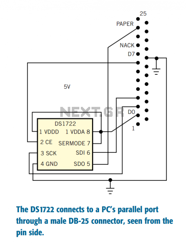
The Dallas Semiconductor DS1722 digital thermometer allows measurement resolution as fine as 0.0625°C in digital form and with linear response. The accuracy specification is only 2°C, but you can improve this figure by careful calibration. Moreover, the accuracy spec...
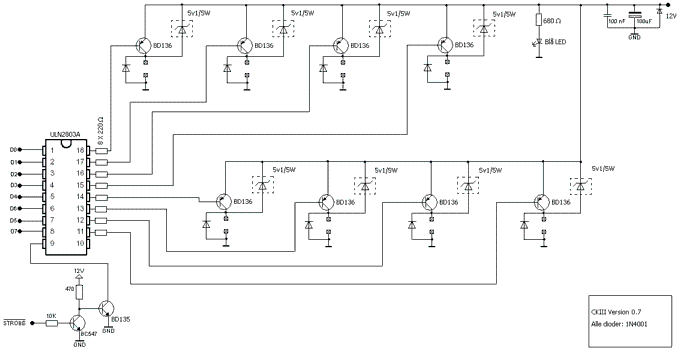
This article was previously published, but the intention is to spread the idea further, potentially inspiring new concepts. An improved version was being developed using an ULN2803A instead of multiple BC547B transistors and optional Zener diodes to ensure that...
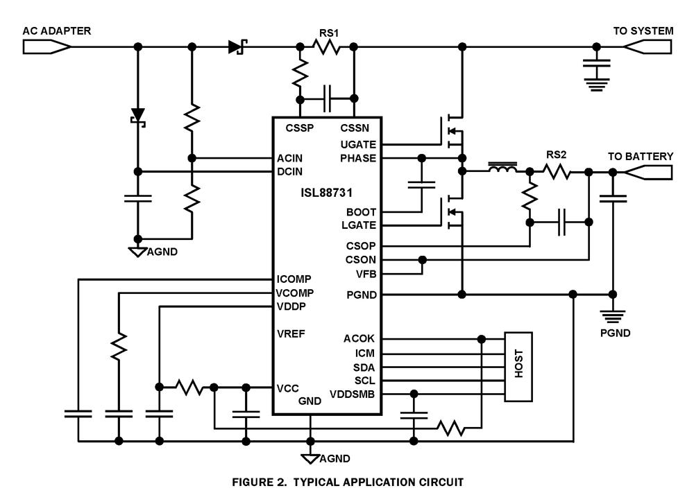
The ISL88731 is a highly integrated Lithium-ion battery charger controller that can be programmed via the SMBus system management bus. It is designed for use in a smart battery charger (SBC) within a smart battery system (SBS) that regulates...

A small ultrasonic cleaning device currently operates with one 50W transducer. There are plans to construct another device using two 20W transducers, and the best configuration for wiring them—either in series or in parallel—is being considered. The circuit designs...