
TV antenna booster

The TV antenna booster circuit employs the BF180 transistor, known for its high-frequency performance, making it suitable for UHF applications. The common base configuration is advantageous in this design as it offers a low input impedance, which is ideal for matching the high-frequency signals typically received by UHF antennas.
The band-pass filter formed by capacitors C2, C3, C4, C5, and inductors L3 and L4 is critical in this circuit. It selectively allows the desired UHF signals to pass while attenuating unwanted frequencies, thus enhancing the overall performance of the antenna system. The gain of 15 dB indicates that the circuit can significantly amplify weak signals, improving the quality of received television broadcasts.
Biasing resistors R2 and R3 ensure that the transistor operates within its optimal range. Proper biasing is essential for maintaining the linearity of the amplifier and preventing distortion of the amplified signal. The circuit's design must also consider power supply decoupling to minimize noise and ensure stable operation under varying load conditions.
Overall, this TV antenna booster circuit is an effective solution for enhancing UHF signal reception, making it a valuable addition to any television setup in areas with weak signal coverage.The circuit shown here is of a TV antenna booster based on the transistor BF180. The circuit operates in the UHF band and has a gain of 15dB. Capacitors C2, C3 C4, C5 and inductors L3, L4 forms a UHF band pass filter. The input signal is fed to the emitter of Q1 through this filter. Resistor R2 and R3 biases the transistor Q1 which is wired in the common base configuration. 🔗 External reference
Related Circuits
The amplifier's gain is nominally 20 dB. Its frequency response is primarily influenced by the values of a few components, mainly C1 and R1. The schematic diagram's component values yield a frequency response of ±3.0 dB from approximately 120...
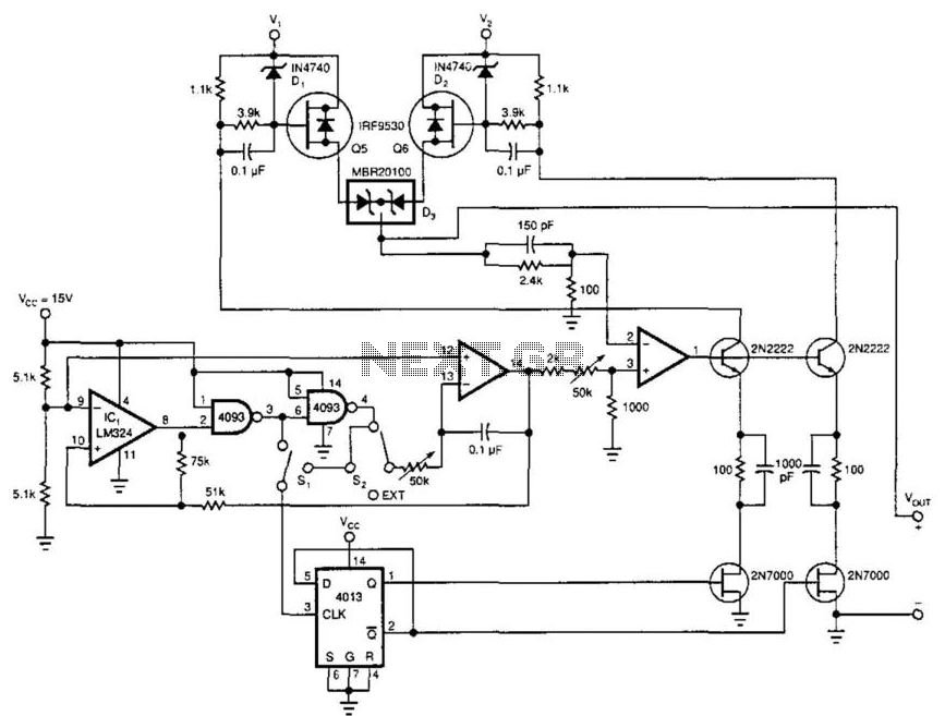
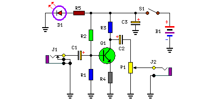
This power booster operates as a high-efficiency power multiplexer or, when supplied with an external signal source, as a high-power linear amplifier. For driving a load with a high-power square wave, the circuit alternately draws power from two external...

This design presents a simple antenna amplifier electronic circuit project, which can be utilized based on the provided circuit diagram. The antenna amplifier operates effectively within a frequency range of 1 to 300 MHz. It is suitable for high...
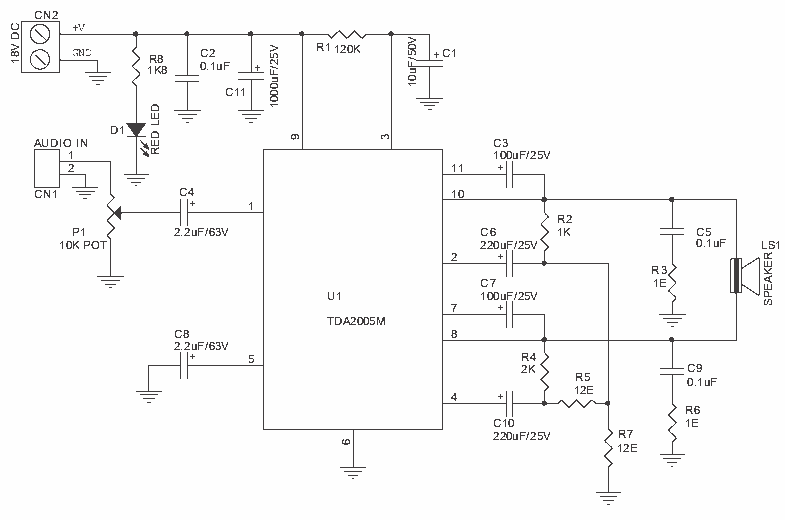
20W Bridge Audio Amplifier kit, based on the TDA2005 IC, a class B dual audio amplifier, specifically designed for car radio applications etc. More: Power supply - 18 VDC Output power - 20 W, 4 Ω IC built in Thermal Shut-down,...
This is a high-performance radio receiver antenna amplifier designed for the entire VHF broadcast and PMR band (100-175 MHz) that can be successfully constructed without... This radio receiver antenna amplifier is engineered to enhance the signal quality and reception capabilities...
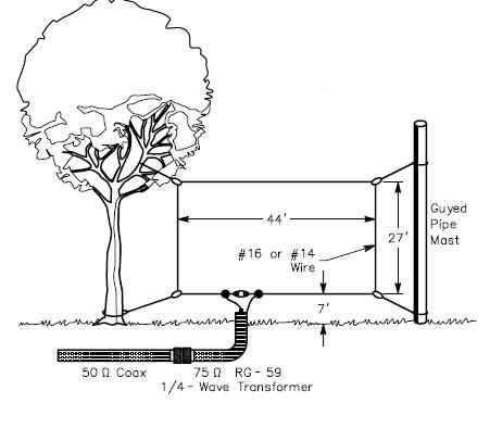
The loop may be fed at the center of one of the vertical sides if vertical polarization is preferred. For horizontal polarization, feeding is necessary at the center of either horizontal side. Optimum directivity occurs at appropriate angles towards...