
Tube for a shunt voltage regulator

The described circuit configuration includes a Field Effect Transistor (FET), a Zener diode, and a resistor, which can be utilized for voltage regulation or signal conditioning applications. The FET serves as a switch or amplifier, while the Zener diode is used for voltage clamping to maintain a stable output voltage regardless of fluctuations in input voltage or load conditions.
In scenarios where the current flowing through the circuit is within the specified limits of the Zener diode, the FET and resistor components can be omitted. This simplifies the design and reduces component count, enhancing reliability and efficiency.
When a P-channel FET is selected, it can be used in high-side switching applications, allowing for control of the load connected to the positive supply voltage. The gate of the P-channel FET is typically connected to a control signal, which, when pulled low, turns on the FET, allowing current to flow from the source to the drain.
For proper operation, it is essential to reference the datasheets of the selected components to ensure they meet the voltage and current requirements of the application. The Zener diode should be chosen based on its reverse breakdown voltage, which must align with the desired output voltage level. The resistor, if utilized, should be calculated to limit the current through the Zener diode to a safe level, ensuring it operates within its specified power dissipation limits.
This configuration can be effectively employed in power supply circuits, signal processing applications, or as a part of more complex electronic systems where voltage regulation is critical. or take one FET, one Zener, and one resistor. No FET and resistor needed if the current is in the range of specs for a zener. Or take a P-channel.. 🔗 External reference
Related Circuits

CRTGND is not equivalent to GND; CRTGND connects to the MOSFET drain or Schottky diode. A disadvantage of this circuit is the voltage drop when powered from the USB side due to the diode. The USB voltage can fluctuate...
Applications include the 900 MHz ISM Band, Satellite TV LNB IF Amplifiers (950 - 2150 MHz), 1575 MHz GPS, 2.4 GHz ISM Band (802.11 b/g WLAN, Cordless, etc.), "SDARS" Satellite-based Radio (2.33 and 2.6 GHz), 5-6 GHz WLAN (802.11a),...

This project is designed to provide security for personal belongings left on a beach towel while swimming or engaging in other activities. The project involves creating a portable electronic alarm system that can be easily set up on a...
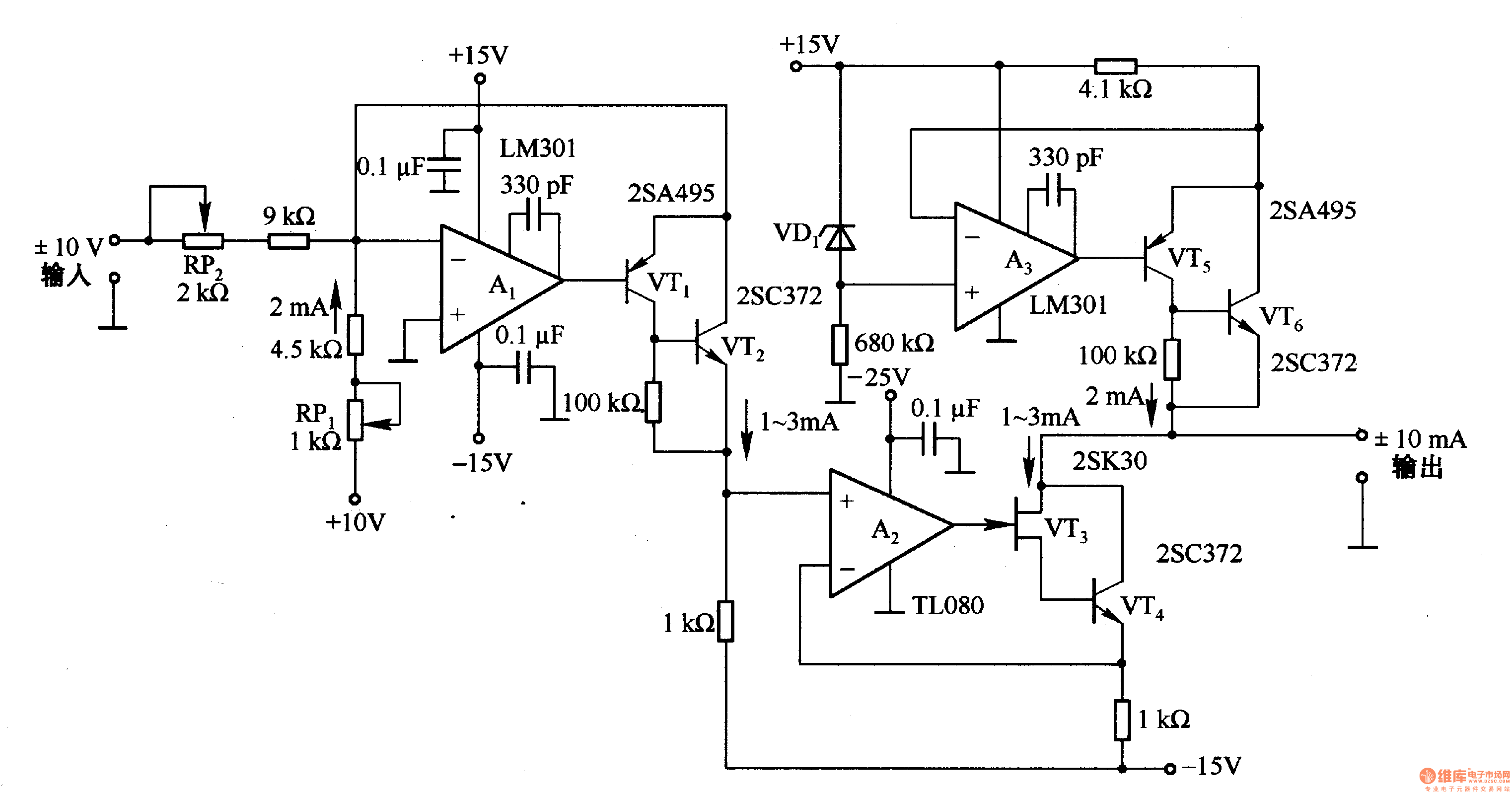
This circuit is designed for voltage-to-current conversion, specifically transforming a ±10V input voltage into a ±1mA output current. The conversion process is facilitated by operational amplifier A1 and transistors VT1 and VT2, which are responsible for altering the current...
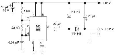
This voltage doubler circuit utilizes a 555 timer integrated circuit configured as an astable multivibrator. It can deliver a maximum output current of 50mA; exceeding this limit will result in a reduction of the output voltage. The actual output...
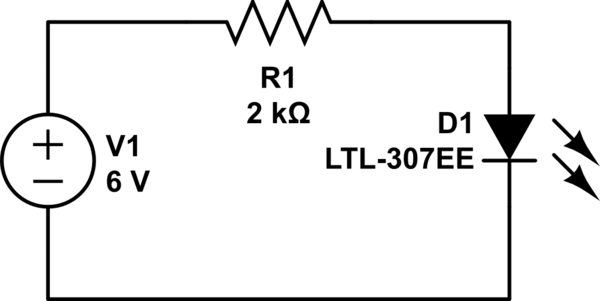
It cannot be 0 volts, as the current does not flow freely due to the presence of the resistor. This results in one side being more negatively charged and the other side more positively charged, as electrons can move...