
high impedance input JFET/BJT buffer circuit
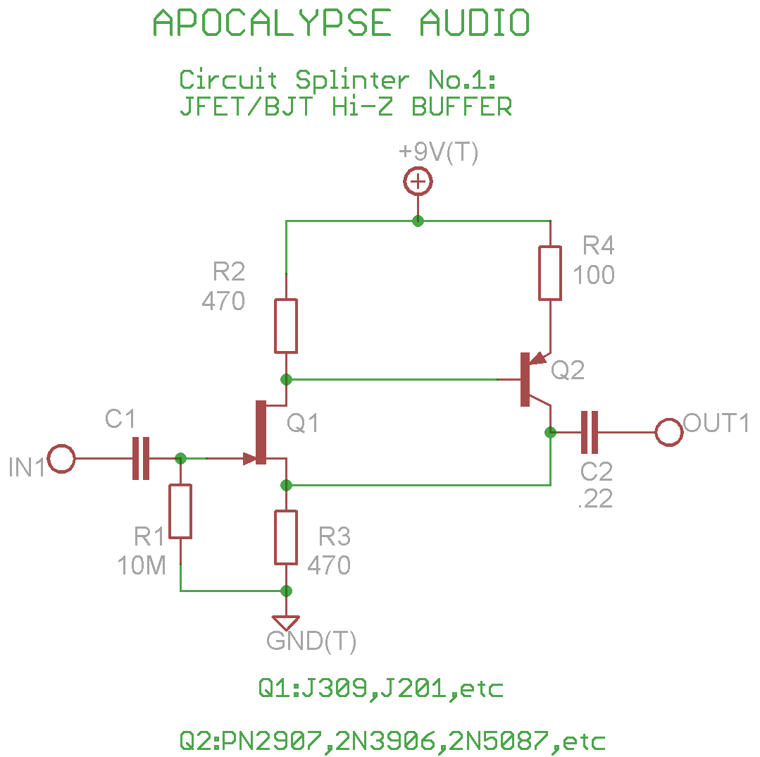
The circuit in question is a hybrid design that effectively combines the characteristics of both JFETs and BJTs to create a versatile audio buffer. The use of an NPN JFET allows for high input impedance, which is critical in audio applications to prevent loading of the previous stage and preserve signal integrity. This high impedance is particularly beneficial for interfacing with high-impedance sources such as electric guitar pickups.
The PNP BJT is configured in an inverted manner, which is essential for compatibility with negative ground systems, commonly found in modern electronic devices. This configuration not only minimizes noise but also enhances the overall performance of the circuit by leveraging the low noise characteristics of the PNP transistor.
The resistor R1 plays a pivotal role in determining the input characteristics of the circuit. By varying its value between 1M and 10M, one can tailor the low-frequency response of the circuit, making it adaptable to different audio signals. The capacitor C1, which is left to the user's discretion, will further influence the frequency response and can be selected based on the desired cutoff frequency for the application.
To transform this buffer into an amplifier, the addition of a feedback resistor in the appropriate location is crucial. This feedback resistor can be connected from the collector of the PNP transistor to its base, creating a negative feedback loop that increases gain while maintaining stability. The specific value of this resistor will determine the gain of the amplifier stage, allowing for customization based on user requirements.
Overall, this circuit not only serves as a buffer but also offers the potential for expansion into more complex audio processing applications, such as a booster or overdrive, making it a valuable addition to any audio engineer's toolkit. Further exploration of this circuit in subsequent discussions will likely yield additional insights and modifications for enhanced performance.this is a rather common cookbook circuit that you can find in books and on the net, yet personally i have yet to see it in stompbox circles, so i thought i would post it. it uses an npn JFET DC coupled with a pnp BJT . the FET allows a a much higher input impedance than a BJT normally would. R1 could realistically be anything from 1M to 10M, this will only really affect the low end coupled with C1(which i have left open for you to decide the value).
the BJT is "inverted" so that a pnp transistor can be used with a negative ground circuit, for what i presume is for it's lower noise specs. i haven't measured the output current of this configuration versus a single FET buffer, but that could be something i'll do in the future and report back.
the real reason i am posting this buffer is because it can easily be turned into an amplifier stage, which can subsequently be used for a sweet booster/overdrive. all that and more in the next installment of CIRCUIT SPLINTERS! bonus question: anyone want to tell me where to place the resistor in order to turn this buffer into an amplifier?
🔗 External reference
Related Circuits

This circuit allows for the adjustment of resistance using a potentiometer and the adjustment of capacitance by opening or closing switches. By manipulating the configuration of these switches, various combinations can be achieved to obtain different effective capacitance values....
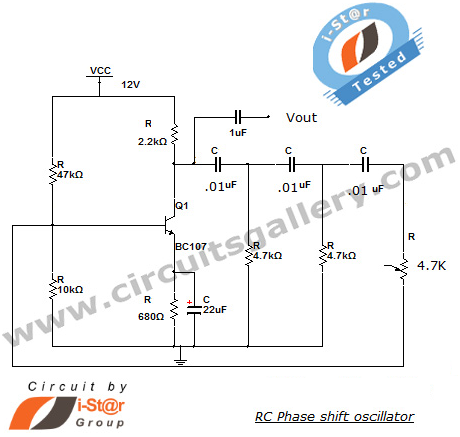
This section introduces a transistor oscillator circuit known as the RC Phase Shift Oscillator. An oscillator is an electronic circuit that functions as a sine wave generator, requiring only a DC power supply. It is commonly used in variable...
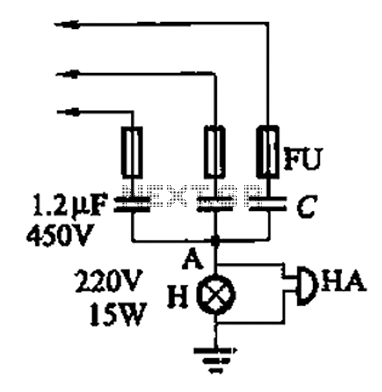
A 3-phase power system poses risks to electrical equipment, particularly asynchronous motors. To detect phase failure, an alarm circuit can be implemented. When the power supply is normal, the voltage at point A is approximately 0V, and no alarm...
The accumulator charger circuit must provide a voltage that matches the specifications of the batteries being charged. For a 12-volt accumulator, the output voltage should not exceed 12 volts, nor should it fall significantly below this threshold. Failure to...
Direct measurement circuit for soil content, assessing various parameters such as moisture, salinity, nitrogen, and pH to enhance soil quality for diverse agricultural crops. This electronic measuring circuit facilitates rapid and accurate testing of soil conditions and informs fertilization...
The following circuit illustrates a Simple Moisture Detector Circuit Diagram. This circuit is based on the 4093 IC. Features include the ability to detect a certain level of moisture. The Simple Moisture Detector Circuit utilizes the 4093 integrated circuit, which...