
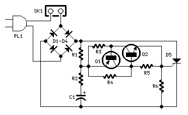
Clap Switch circuit diagram

The clap switch circuit utilizes a combination of analog and digital components to effectively respond to sound input. The condenser microphone serves as the primary sensor, converting acoustic energy from claps into an electrical signal. This signal is then amplified by transistor T1, ensuring that even soft claps are detected reliably. The design incorporates two integrated circuits, IC1 and IC2, which are crucial for timing and triggering functions. IC1's monostable configuration ensures that the circuit remains responsive only for a defined period after the first clap, thus preventing accidental activation from extraneous noise.
The timing elements, R7 and C3, are selected based on the desired response time. The relationship between resistance and capacitance allows for flexibility in tuning the circuit to specific applications. The second clap triggers IC2, which is responsible for generating the output that activates the relay. The decade counter IC 4017 is utilized in a bistable mode to maintain the state of the relay, providing a stable on/off control for the connected appliance.
The use of a free-wheeling diode (D1) is essential in inductive load applications, as it protects the transistor from voltage spikes caused by the collapsing magnetic field of the relay coil. This safeguard enhances the longevity and reliability of the circuit. Additionally, the inclusion of indicator LEDs (LED1 and LED2) provides visual feedback to the user, confirming the operational status of the system. Overall, this clap switch design is an efficient and user-friendly solution for remote control of electrical devices, leveraging simple yet effective electronic principles.Here`s a clap switch free from false triggering. To turn on/off any appliance, you just have to clap twice. The circuit changes its output state only when you clap twice within the set time period. Here, you`ve to clap within 3 seconds. The clap sound sensed by condenser microphone is amplified by transistor T1. The amplified signal provides negat ive pulse to pin 2 of IC1 and IC2, triggering both the ICs. IC1, commonly used as a timer, is wired here as a monostable multivibrator. Trigging of IC1 causes pin 3 to go high and it remains high for a certain time period depending on the selected values of R7 and C3. This on` time (T) of IC1 can be calculated using the following relationship: T=1. 1R7. C3 seconds where R7 is in ohms and C3 in microfarads. On first clap, output pin 3 of IC1 goes high and remains in this standby position for the preset time.
Also, LED1 glows for this period. The output of IC1 provides supply voltage to IC2 at its pins 8 and 4. Now IC2 is ready to receive the triggering signal. Resistor R10 and capacitor C7 connected to pin 4 of IC2 prevent false triggering when IC1 provides the supply voltage to IC2 at first clap. On second clap, a negative pulse triggers IC2 and its output pin 3 goes high for a time period depending on R9 and C5.
This provides a positive pulse at clock pin 14 of decade counter IC 4017 (IC3). Decade counter IC3 is wired here as a bistable. Each pulse applied at clock pin 14 changes the output state at pin 2 (Q1) of IC3 because Q2 is connected to reset pin 15. The high output at pin 2 drives transistor T2 and also energizes relay RL1. LED2 indicates activation of relay RL1 and on/off status of the appliance. A free-wheeling diode (D1) prevents damage of T2 when relay de-energizes. 🔗 External reference
Related Circuits
This is a 220V LED flasher circuit designed as a reliable alternative to thermally activated switches used for flashing Christmas tree lamps. It is a cost-effective and easy-to-assemble circuit. The components include R1 (100K), R2 (1K), R5 (1K), R3...
Both circuits can synchronize trapezoidal wave voltage, which is converted into intermittent small rectangular pulses. Its working principle involves periodic operation in synchronization with the grid frequency of the zero-volt switching voltage of the DC chopper. Due to the...
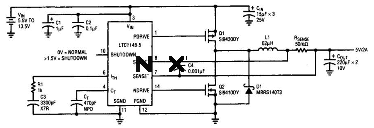
A typical LTC 1148 surface-mount application provides 5 V at 2 A from an input voltage range of 5.5 V to 13.5 V. The operating efficiency, illustrated in B, peaks at 97% and remains above 90% from 10 mA...
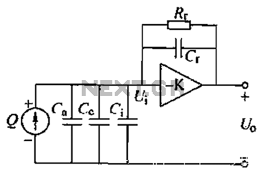
A charge amplifier is an effective device for measuring punch hits. This amplifier utilizes a negative feedback capacitor in conjunction with a high-gain operational amplifier. The amplifier operates with minimal shunt, relying primarily on the feedback capacitor's charge (q...
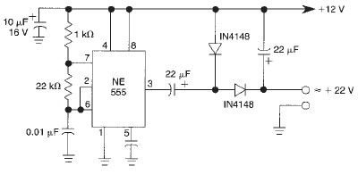
This voltage doubler circuit utilizes a 555 timer integrated circuit configured as an astable multivibrator. It can deliver a maximum output current of 50mA; exceeding this limit will result in a reduction of the output voltage. The actual output...
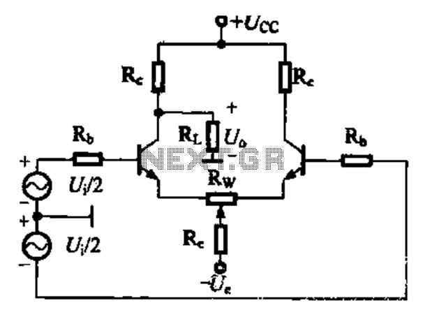
A comparison of four connection methods and features of a differential amplifier circuit is presented. The circuit demonstrates a magnification of a single tube with half the earnings, effectively countering common-mode negative feedback effects. The Common-Mode Rejection Ratio (CMRR)...