
CMOS and PMOS cross interface circuit b

The CMOS and PMOS cross interface circuit is designed to facilitate seamless communication between CMOS (Complementary Metal-Oxide-Semiconductor) and PMOS (P-channel Metal-Oxide-Semiconductor) technologies. The primary advantage of utilizing PMOS in this configuration is its high input impedance, which results in minimal loading on preceding stages of the circuit. This characteristic is particularly beneficial in applications where signal integrity is paramount, as it ensures that the input current can be effectively ignored, thereby preserving the original signal characteristics.
In the schematic representation of the circuit, the PMOS transistors are typically arranged in a manner that allows them to interface effectively with CMOS logic levels. The circuit may incorporate level-shifting mechanisms to accommodate the different voltage levels inherent in CMOS and PMOS technologies. This ensures compatibility and reliable operation across various parts of the system.
The design may also include pull-up or pull-down resistors to maintain the desired logic levels during transitions. Additionally, capacitive coupling may be employed to filter out noise and stabilize the input signals. The careful selection of component values is crucial to achieve the desired performance metrics, including switching speed, power consumption, and thermal stability.
Overall, the CMOS and PMOS cross interface circuit is a vital component in mixed-signal applications, enabling efficient signal processing and interfacing between different semiconductor technologies while maintaining high fidelity and low power consumption. CMOS and PMOS cross interface circuit b PMOS integrated circuit high input impedance, input current can be ignored. CMOS and PMOS interface circuit shown in Figure
Related Circuits

A resistor R1, capacitor C1, and two converters create a square wave generator that produces a fundamental tone. This generator is followed by an inverter that functions as both a buffer and a driver for the system. Resistor R2,...

This is a cost-effective and straightforward emergency light circuit developed for CircuitsToday. It is an automatic emergency lamp with daylight sensing capabilities, meaning it detects darkness and turns on automatically, while also sensing daylight to turn off. The circuit...

This keyer utilizes skin conductivity to emulate the traditional mechanical CW bug keyer. When the dit paddle is activated, the bias on the inverter, IC1-a, is routed to ground, resulting in a logic high output. This triggers oscillator sections...

This circuit requires physical connections to be made to the computer's serial port (COM1 or COM2). It is generally considered difficult to cause harm to oneself or the computer through improper connections to this port; however, there is no...

This design note presents a simple yet feature-rich 16-watt output, universal AC input adapter power supply for modems, hubs, or similar applications. The circuit utilizes a discontinuous mode (DCM) flyback converter topology designed around ON Semiconductor's NCP1027 monolithic current...
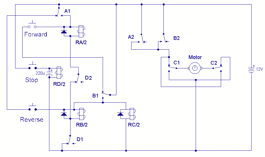
A DC motor reversing circuit using non-latching push button switches. Relays control forward, stop, and reverse action, and the motor cannot be switched from forward to reverse unless the stop switch is pressed first. The described circuit employs a system...