
CMOS interface circuit with the PMOS cross-c

The CMOS interface circuit utilizing PMOS cross-coupled configurations is designed to achieve high input impedance, making it suitable for applications where minimal loading on the preceding stage is critical. The PMOS transistors in this configuration operate in a complementary manner, allowing for enhanced performance in terms of noise margins and power consumption.
In this circuit, the PMOS transistors are arranged in a cross-coupled manner, which provides improved stability and reduces the susceptibility to variations in temperature and supply voltage. The high input impedance characteristic of this configuration is primarily due to the inherent properties of PMOS transistors, which exhibit low gate leakage currents. Consequently, the input current can be considered negligible, allowing for accurate signal processing without significant distortion or attenuation.
The CMOS interface circuit can be employed in various applications, including analog signal processing, sensor interfacing, and as part of more complex digital systems. The circuit's design typically includes biasing networks to ensure optimal operating conditions for the PMOS devices, as well as decoupling capacitors to filter out noise from the power supply.
In summary, the described CMOS interface circuit with PMOS cross-coupled transistors provides a robust solution for interfacing high-impedance sources while maintaining low power consumption and high signal integrity, making it an essential component in modern electronic designs. CMOS interface circuit with the PMOS cross-c PMOS integrated circuit high input impedance, input current can be ignored. CMOS and PMOS interface circuit shown in Figure
Related Circuits

The circuit depicted in the figure is a generator that includes an oscillator, a voltage follower, a zero amplitude adjustment, and a zero shift circuit. It is utilized as a self-balancing recorder for testing signals. The output signal ranges...
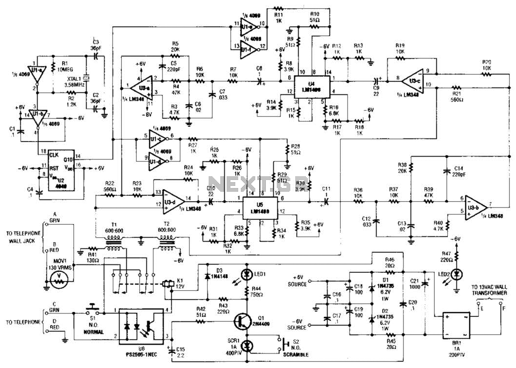
Two hybrids (T1 and T2) are utilized to facilitate a direct connection to a telephone line. This circuit employs a standard speech-inversion algorithm, which inverts the frequency of an audio signal around a central frequency. An LM1496 balanced modulator...

The CD4001 quad 2-input NOR gate is a highly versatile integrated circuit (IC) that can be utilized in numerous applications. This example demonstrates its use in a simple alarm system. The recommended power supply voltage for the CD4001 ranges...
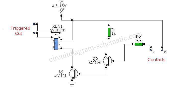
The circuit diagram represents a water-activated relay circuit. This circuit employs two transistors configured as a high-gain compound pair. The transistors used are 2N2222A for T1 and T2, which may also be substituted with BC108. The current gain is...
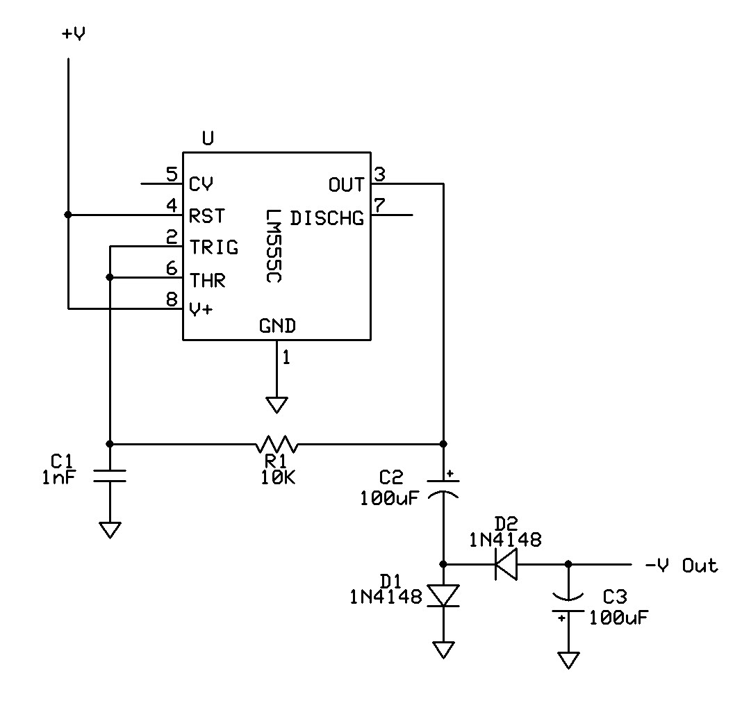
Can a 555 negative supply circuit, like the one below I pulled from another schematic, supply enough negative voltage to an LM324 and an AD736JN? The 555 timer integrated circuit can be configured to generate a negative voltage supply,...

The digital display temperature detection circuit utilizes a precision digital display to indicate temperature readings. The circuit employs the MC1403, which outputs a reference voltage, with the potentiometer RP5 setting the reference value for the inverting terminal (a) of...