
Correct Board Layout Lowers EMI of Switchmode Converters
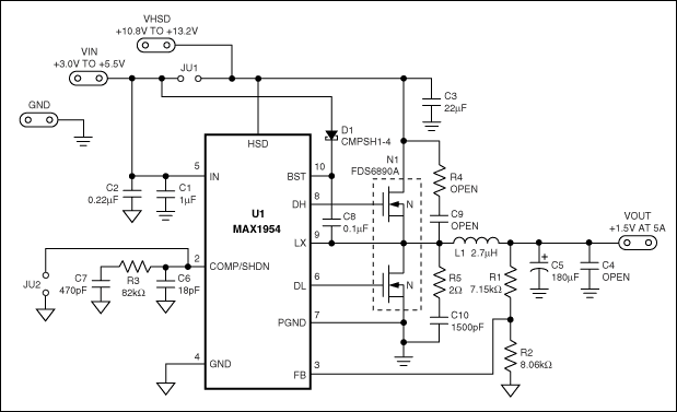
The layout of switch-mode DC-DC converter PCBs is critical in ensuring efficient operation and compliance with electromagnetic compatibility (EMC) standards. Key factors to consider include the placement of components, routing of traces, and the design of ground planes.
1. **Component Placement**: Components should be arranged to minimize the loop area of high-frequency current paths. The input and output capacitors should be placed as close as possible to the switching device to reduce parasitic inductance. Additionally, the placement of inductors and transformers should be optimized to prevent coupling of magnetic fields that can induce noise in adjacent circuits.
2. **Trace Routing**: High-frequency switching paths should be kept short and direct. Power traces must be wide enough to handle the current without excessive voltage drop or heating. It is advisable to use a star ground configuration to avoid ground loops, ensuring that return paths for high-frequency currents do not interfere with sensitive analog or digital signals.
3. **Ground Planes**: A solid ground plane is essential for minimizing EMI. The ground plane should be continuous and unbroken, providing a low-impedance return path for high-frequency currents. If multiple ground levels are necessary (e.g., digital and analog grounds), they should be connected at a single point to prevent ground loops.
4. **Decoupling Capacitors**: Placing decoupling capacitors as close as possible to the power pins of integrated circuits (ICs) helps to filter out high-frequency noise. The selection of capacitor types (ceramic, tantalum, etc.) and values should be based on the frequency characteristics of the circuit.
5. **Shielding and Filtering**: In cases where EMI is a significant concern, additional measures such as shielding enclosures or ferrite beads on power lines may be employed. Filters can also be integrated into the design to attenuate unwanted frequencies.
By adhering to these layout principles, the performance of switch-mode DC-DC converters can be optimized, leading to reduced noise and improved reliability in various applications.Describes how to layout switch-mode DC-DC converter printed circuit boards (PCBs) to minimize switching noise and EMI.. 🔗 External reference
Related Circuits
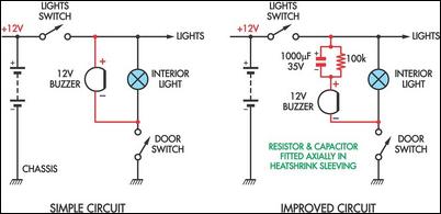
Two headlight reminder circuits are simple to install and operate based on the KISS (Keep It Simple Stupid) principle. The basic circuit consists of a 12V piezo buzzer connected between the lights circuit and a door switch. The buzzer...

The circuit operates using AC mains voltage and other high voltages that pose risks of injury or death. The 125 employs a basic heterodyne configuration, where the outputs of two similar radio-frequency Colpitts oscillators are fed into a mixer,...
The wire connected to the 5V pin is linked to the positive pins of the breadboard, which are not connected to any other components. There are no additional connections on the positive column. While this may seem like a...

This circuit operates at or near series resonance. It is a well-designed circuit with no parasitics. It is easy to tune and has good frequency stability. The circuit in question utilizes series resonance to achieve optimal performance. At series resonance,...

The microcontroller is an AT90S8535-P in a DIP40 package. It is pin-compatible with other members of the AVR analog series, such as the ATMega8535 and ATMega16, although there are significant differences among them. It is advisable to consult the...
The PWM pulse width modulation controller board enables 9S12/HCS12 microcontrollers or PIC microcontrollers to output 8 channels, each capable of delivering 5 DC amps, while incorporating current sensing for the PWM waveform. This PWM driver circuit is suitable for...
Warning: include(partials/cookie-banner.php): Failed to open stream: Permission denied in /var/www/html/nextgr/view-circuit.php on line 713
Warning: include(): Failed opening 'partials/cookie-banner.php' for inclusion (include_path='.:/usr/share/php') in /var/www/html/nextgr/view-circuit.php on line 713