
D A conversion frequency generator complementary bipolar

The AD7520 integrated circuit is designed for applications requiring precise digital-to-analog conversion across multiple channels. Each of the 10 channels operates independently, allowing for versatile signal generation in various electronic systems. The DAC utilizes a CMOS architecture, which contributes to low power consumption and high speed, making it suitable for battery-powered devices.
The operation of the circuit begins with the input current Io1 being converted into a corresponding digital output. This digital output is represented by N bits, where N can vary based on the specific application requirements. The additional output proportional to Io2, calculated as (1023-N), allows for further manipulation of the signal, providing a dual output capability that enhances the versatility of the circuit.
The inclusion of the LF353N operational amplifier ensures that the output signal is amplified appropriately, maintaining signal integrity throughout the conversion process. Capacitors C1 and C2 play a critical role in timing and voltage regulation. The 556 timer, when triggered by the voltage levels across these capacitors, facilitates a reset mechanism that is essential for maintaining consistent operation and preventing signal distortion.
The frequency output range of 10 to 10,000 Hz indicates the circuit's capability to handle various signal types, making it suitable for audio applications, control systems, and other dynamic signal processing tasks. The adjustment of frequency via RP1 allows for fine-tuning of the output to meet specific application needs.
Overall, the AD7520 circuit exemplifies a robust solution for digital-to-analog conversion, with features that cater to a wide range of electronic applications, ensuring precise control and adaptability in signal generation. As shown in FIG, AD7520 is a CMOS type integrated circuit DAC over 10 channel, may be provided with l0 N-bit digital output proportional to the input current Io1, it offers the (1023-N) proportional to the current Io2. VT1, VT2 and broadband dual op amp LF353N capacitor C1, C2 charging current. When the charging voltage of C1, C2 reaches the threshold level when the 2/3 VDD, 556 reset; C1, C2 through the inner discharge tube discharge substrate corresponding to 1/3 VDD, then set to and is proportional to N the Io1 and rate Io2 and (1023-N) is proportional to recharge the battery. Because Io1 digital proportional to N, so the availability of l0 ~ 10000Hz frequency output. 555 provides the pulse and sawtooth output simultaneously. RP1 is used to adjust the frequency range.
Related Circuits
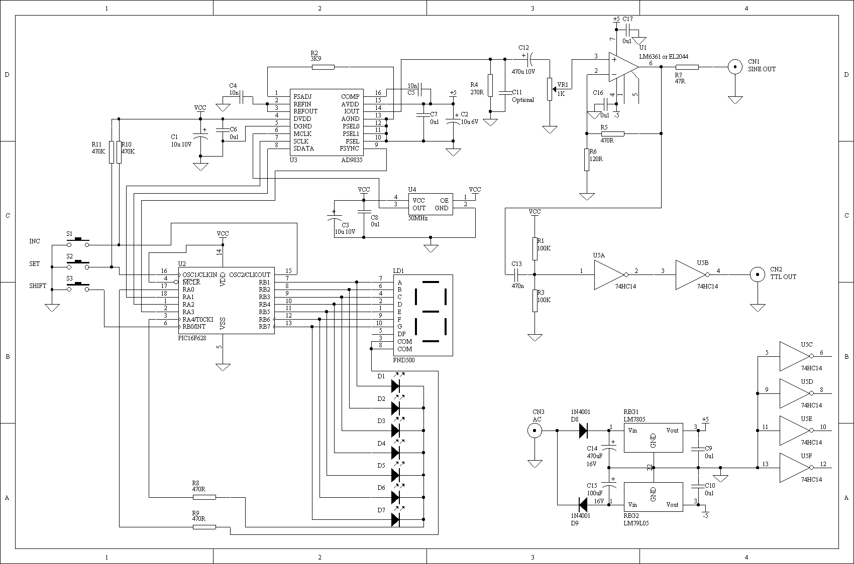
An extremely simple and low cost Sine/Square wave generator based on the Analog Devices AD9835 Direct Digital Synthesis (DDS) Generator chip. The frequency can be set for any frequency from 1Hz to 10MHz in 1Hz resolution steps! All this...
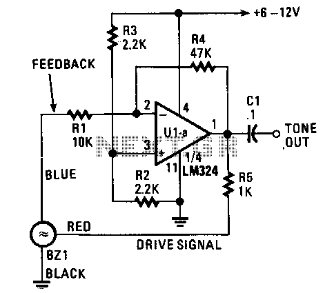
A single operational amplifier, one-fourth of an LM324 quad op-amp, is configured as a standard inverting amplifier. Upon power-up, a positive voltage is applied to the non-inverting input of U1 through resistor R3, which drives its output high. This...
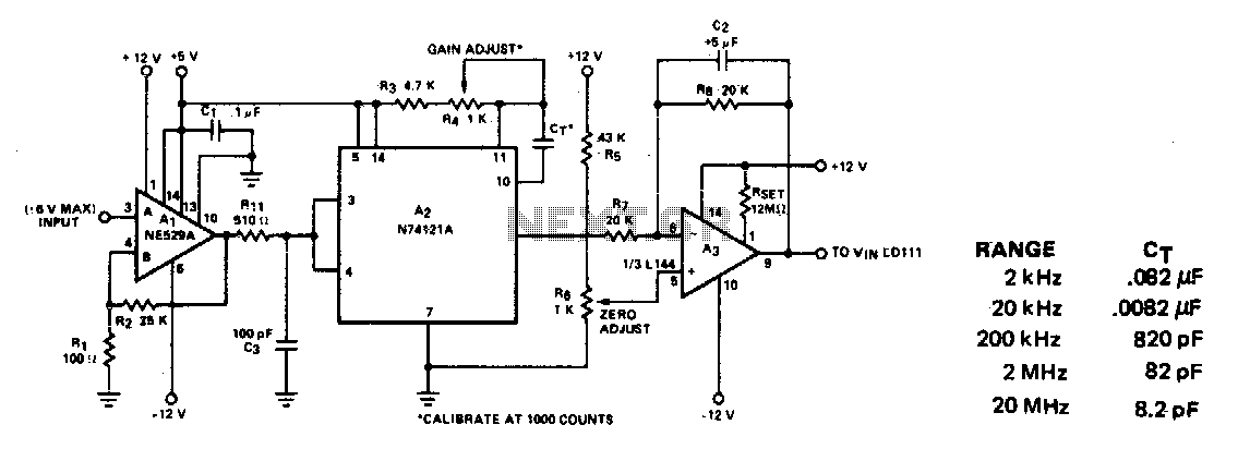
This circuit converts frequency to voltage by taking the average DC value of the pulses from the 74121 monostable multivibrator. The one-shot is triggered by the positive-going AC signal at the input of the 529 comparator. The amplifier acts...
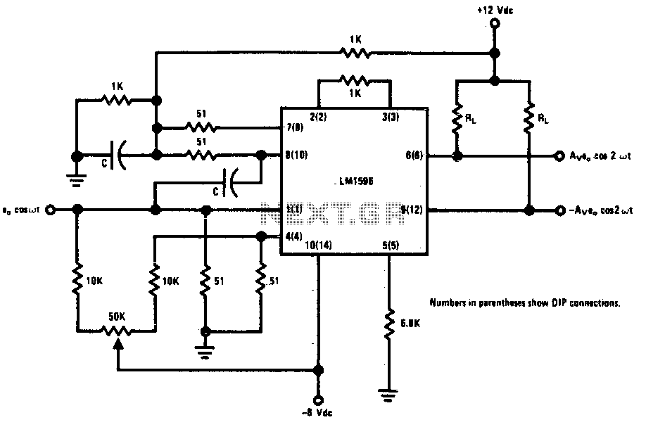
This circuit is designed to double low-level signals while maintaining low distortion. The capacitor value (C) should be selected to ensure low reactance at the operating frequency. The signal level at the carrier input should remain below 25 mV...
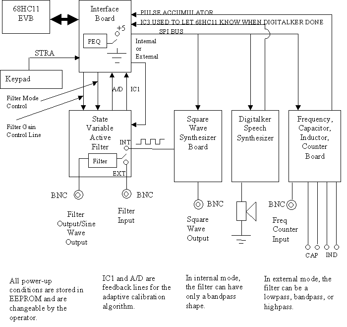
This site contains complete schematics and code for a 68HC11 based frequency counter, square wave synthesizer, sine wave synthesizer, programmable filter, capacitance and inductance meter, with a digitalker speech synthesizer output. Project specifications are given below. The project outlined involves...
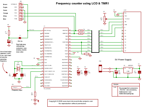
C code for a PIC frequency counter operating up to approximately 50 MHz. The project utilizes an HD47880 LCD for display purposes and employs Timer 1 to count the edges of the input signal. This frequency counter project is designed...