
DA-101 FM radio circuit chip

FM radio chip circuits, such as the one utilizing the DA-101 chip, are designed to receive and process FM radio signals effectively. The circuit operates by using a headset jack as an antenna, allowing for the capture of FM broadcasts. The initial signal captured is passed through coupling capacitor C58, which serves to filter and couple the radio frequency signal into the U13 chip.
Once the signal reaches U13, it undergoes several stages of processing. The first stage is high-frequency amplification, which boosts the strength of the received signal to ensure adequate processing. Following this, the signal is mixed, which involves combining it with a local oscillator frequency to convert it to an intermediate frequency (IF). This IF signal is then amplified further to improve clarity and reduce noise.
The output from pin U13 is the audio signal that has been demodulated from the original radio frequency carrier. This audio signal is directed to a digital decoder chip, which translates the audio data into a format suitable for playback or further processing. This integration of digital decoding allows for enhanced audio quality and compatibility with various playback devices.
Control of the radio circuit is managed by a CPU through the I2C bus interface. The CPU sends control signals, including data and clock signals, to the appropriate pins on U13 to facilitate operation. This digital communication allows for precise control over the radio's functions, such as tuning and volume adjustments.
Furthermore, the power management of the U13 chip is crucial for efficient operation. The CPU sends a control signal to gate VT5, which acts as a switch to manage the power supply to U13. By controlling VT5, the CPU can turn the power supply on or off, effectively managing the power consumption of the radio circuit and ensuring that it operates only when necessary. This design consideration enhances the overall efficiency and longevity of the FM radio circuit.Radio FM radio chip circuits use different, it works slightly different, as shown in the use of DA-101 chip FM Figure radio circuit. FM radio broadcast program in the state of the headset as an antenna jack FM radio circuit, the signal received by the antenna coupling capacitor c58 into the U13 @ feet. This signal is a radio frequency carrier. U13 carried out in high-frequency amplification, mixer, IF amplifier, frequency and other processing solutions to bring up the audio signal by , @ pin output, and then sent to a digital decoder chip for processing, radio circuit U13 k {JI as by CPU control, Izc bus control signal to the CPU (DATA, CLK) are applied to the U13 , feet.
Ul3 the radio power supply control signal is a control signal from the CPU applied to the gate VT5 by VT5 applied to the control power supply U13, so as to control the radio purposes.
Related Circuits
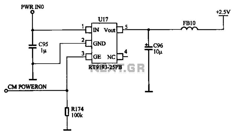
The camera power supply circuit illustrates the essential power supply required for the proper functioning of the camera. This power supply circuit is composed of a stable voltage control integrated circuit. The camera power supply circuit is critical for ensuring...
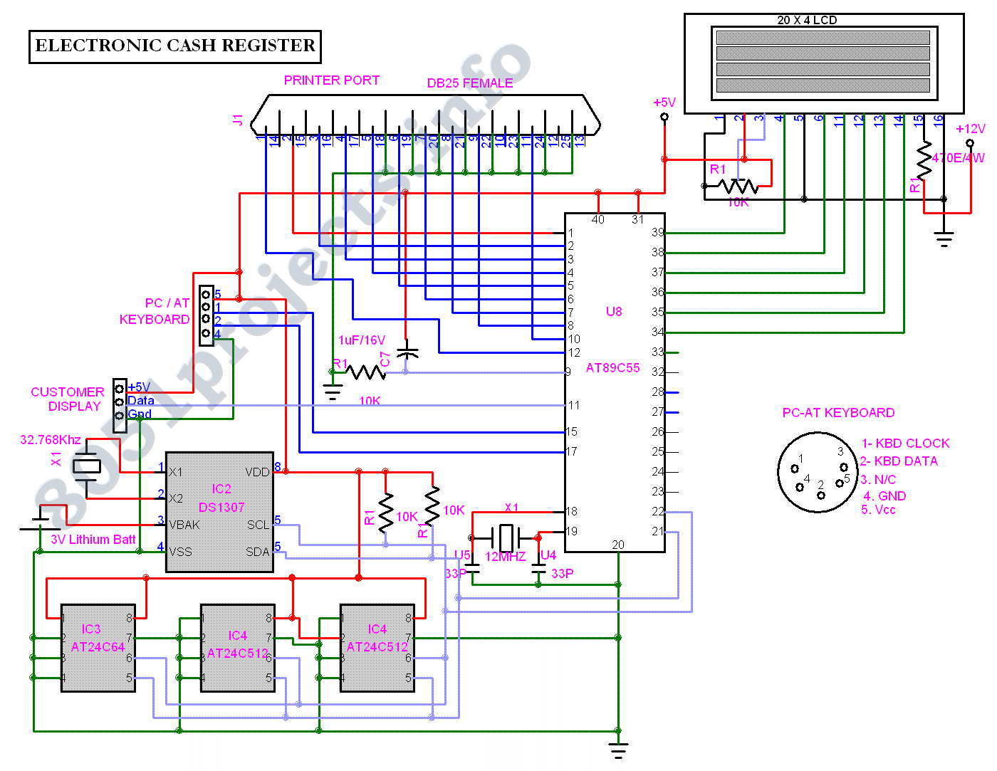
The Electronic Cash Register (ECR) keeps track of sales transactions quickly and effectively. An abundance of PLUs (Price Look Ups) and department keys accommodate a variety of merchandise items. This means a faster, more accurate check out process and...

The output frequency alternates between approximately 2100 Hz and 2200 Hz. This unique test signal is easily distinguishable from other potential signals. Resistor R6 is connected to a wire, approximately ten centimeters long, which serves as the antenna. The...
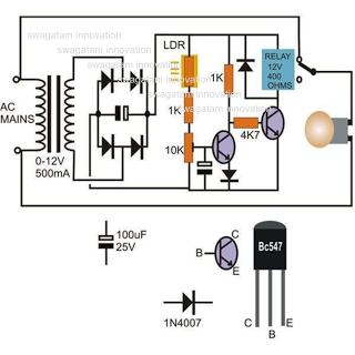
This circuit diagram illustrates a light-activated switch utilizing the National Semiconductor comparator IC LM311 and a light-dependent resistor (LDR). The configuration is based on a voltage comparator circuit centered around IC1. The non-inverting input of IC1 receives a reference...

This circuit is designed for an RF (radio frequency) transmitter experiment, where a watt meter is instrumental in optimizing the transmitter circuit. A simple RF watt meter circuit is illustrated in the schematic diagram below. The circuit is not...

There are two regulator circuits that utilize the L200 integrated circuit from SGS-Thomson to regulate voltage and current. In circuit Fig. 1, the output voltage can be adjusted using the variable resistor RV1. In Fig. 2, both output voltage...