
Days to TN-1 Intelligent negative pulse charging circuit

The TN-1 Intelligent Negative Pulse Charging Circuit is engineered to optimize battery performance through a carefully structured pulse charging methodology. The use of a half-bridge configuration allows for efficient energy transfer and management within the circuit. The discharge switch, Q6, serves a critical function in maintaining the integrity of the battery by preventing unintended discharges, thus ensuring that energy is conserved effectively during the charging process.
The Darlington pair formed by Q5 and Q6 amplifies the control signals, allowing for more precise management of the discharge and charge cycles. This arrangement is particularly beneficial in applications where rapid switching and high current handling are required. The integration of IC3, along with components C and D, provides a robust framework for controlling the pulse generation, thereby allowing for the modulation of the charging process based on real-time feedback from the battery's state.
The oscillator design, utilizing resistors and capacitors to establish time constants, ensures that the charging pulses are delivered in a manner that enhances battery chemistry, promoting better charge acceptance and reducing thermal stress. This is crucial for prolonging battery life and maintaining performance standards, especially in applications where batteries are subjected to frequent charge and discharge cycles.
In conclusion, the TN-1 Intelligent Negative Pulse Charging Circuit represents a significant advancement in battery charging technology, combining sophisticated control mechanisms with efficient energy management to deliver superior charging performance while safeguarding battery health.Days to TN-1 Intelligent negative pulse charging circuit Is a day to TN-I intelligent negative pulse charging circuit. This charger is the main part of the typical half-bridge two chargers, and FIG constituting 2-75 charger circuit is basically the same. This introduces negative pulse charging circuit works. This part of the circuit by the discharge switch, the negative load control pulse, the pulse oscillator consists of three parts. Discharge switch is transistor Q6. Q6 is avoided, the collector and emitter of the battery short circuit, battery discharge. Q6 is turned off, the battery charge to restore power. Q5 and Q6 are directly coupled, commonly known as Darlington. Q6 by loading negative pulse oscillator and joint control. Negative pulse load is controlled by IC3 composed of C and D, D connected to the inverter (circuit in parallel with the two input NAND gate as a NAND gate), only two inputs C are high level, feet is low, the D-inverting make Q6 is turned on, the battery to discharge.
C feet from the multivibrator 1 per second (pulse width 3 ms) positive pulse, C of O feet from the current detection circuit of IC2 O feet, constant current charging O feet high almost electric. In this case, negative pulse to work. Pulse oscillator A and B by the IC3 and C24, C25, two 100 k: C1 resistor constitute a typical multi-harmonic oscillator, charge and discharge time constants different high 3 ms, low 1250 ms.
Negative pulse charging can be improved charge acceptance, reduce the charge temperature. Said charger during discharge, do not turn off the charging circuit.
Related Circuits
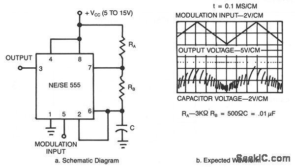
This application utilizes a timer configured for astable (free-running) operation, with a modulating signal applied to the control voltage terminal. The pulse position changes in accordance with the modulating signal, as both the threshold voltage and the time delay...
The typical BPM range for music is between 40 and 240 BPM, corresponding to periods of 1500 ms and 200 ms, respectively. A BPM of 120 equates to a period of 500 ms. The circuit requires a resistor R4...
This inverter circuit is designed to power electric razors, stroboscopes, flash tubes, and small fluorescent lamps using a 12-volt car battery. Unlike conventional feedback oscillator inverters, this design features a separate oscillator from the output stage, allowing for easy...
The circuit does not fail under slight variations, even if the input/output electric current characteristics are exceeded. Failure occurs only during a short circuit or extreme conditions at the output. The operation of the circuit is explained as follows:...
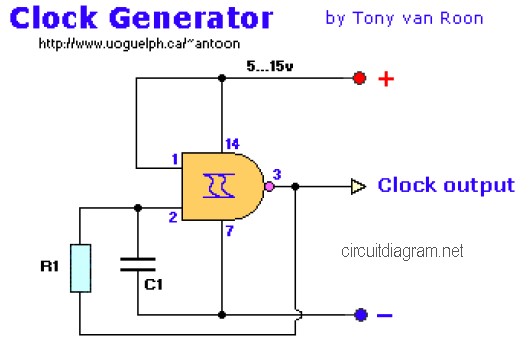
The following diagram is the clock generator circuit diagram built using NAND gate logic integrated circuits (ICs). The circuit can utilize either the IC 7400, which is a TTL type, or the IC 4011, which is a CMOS type....

A compact audio amplifier circuit utilizing the TDA 7052 integrated circuit from Philips. This circuit is suitable for use as a pocket radio amplifier, delivering an output power of 2 watts. The TDA 7052 is a low-voltage audio amplifier designed...