
dc power delay based on scr

The described DC power delay circuit effectively employs an SCR to manage the timing of power delivery in various electronic applications. The key components include capacitor C2, which plays a critical role in storing energy, and resistor R2, which controls the charging rate of the capacitor. The Zener diode D3 is crucial for establishing the voltage threshold that initiates the SCR's conduction.
In operation, upon the application of input voltage, capacitor C2 begins to charge through resistor R2. The time it takes for C2 to reach the necessary voltage level is determined by the values of R2 and C2, which set the RC time constant. Once the voltage across C2 surpasses the Zener breakdown voltage, D3 conducts, providing a gate trigger to SCR H1. This action allows current to flow from the power source to the output, effectively creating a delay in power availability at OUT.
The circuit's delay can be adjusted by modifying the resistance of R2 or the capacitance of C2, enabling customization for specific applications. This flexibility makes the SCR-based DC power delay circuit suitable for use in various electronic devices, such as soft-start circuits in motors, timing applications, and remote control systems, where delayed activation is desirable. Overall, this circuit exemplifies a simple yet effective means of controlling power delivery in electronic systems.The circuit diagram shown here is a simple circuit DC power delay, which is based on an SCR (Silicon-Controlled Rectifier). This circuit is very useful and can be used in many applications. The operation of this circuit is very simple. When input power is applied to the capacitor C2 charges through resistor R2 when the voltage on the capacitor jus
t above the voltage of the Zener diodes D3 breaks, breaks and H1 SCR is triggered and the power delay will be available in late OUT. 🔗 External reference
Related Circuits
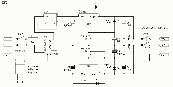
The power supply is based on the LM317 and LM337 variable 3-terminal regulators ICs, and while it is no powerhouse, it is quite satisfactory for testing most power amps, as long as there is no speaker connected. The circuit utilizes...
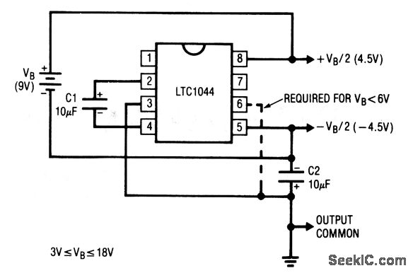
This circuit generates symmetrical ±output voltages, each equal to one-half of the input voltage (for example, a single 9-V battery). The output voltages are referenced to pin 3, which serves as the output common. The circuit is compatible with...
Power line fluctuations and cut-offs can damage electrical appliances connected to the line, particularly domestic appliances such as refrigerators and air conditioners. Operating a refrigerator on low voltage can lead to excessive current flowing through the motor, resulting in...
The following diagram illustrates a 50W offline switching power supply circuit design. This circuit is powered by a MOSFET, specifically the BUZ80A/IXTP4N8 for a 220V AC voltage input and the GE IRF823 for a 110V AC voltage input. The...
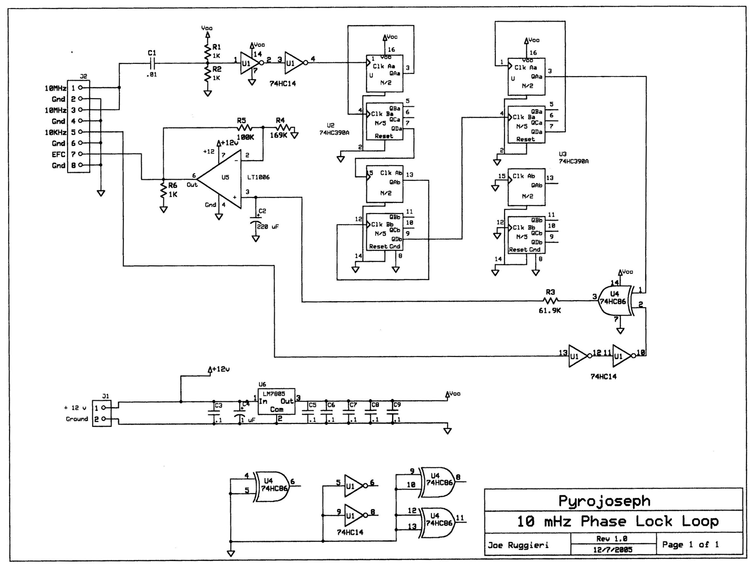
The block diagram illustrates that a 10 MHz signal is generated by an oven-stabilized 10 MHz crystal oscillator, which is locked to a precision 10 kHz signal produced by a GPS receiver module through a phase-locked-loop (PLL) circuit. In...
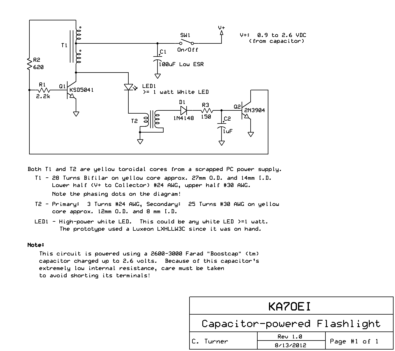
High-energy capacitors can produce hundreds of amps when short-circuited, potentially causing severe burns, fires, and property damage. It is essential to be aware of these hazards when using such capacitors and to take precautions to avoid accidental short-circuits. The...