
Delay circuit with NE555 timer

This circuit employs a simple delay mechanism to control the activation of a device through an LED photocell arrangement, utilizing an optocoupler for isolation between the control and power circuits. The primary components involved in this design include a resistor (R1), a capacitor (C1), a zener diode (D1), and a transistor (Q1).
The operation begins with capacitor C1 charging through resistor R1 when power is applied. The circuit is designed for a nominal supply voltage of 12 volts. As C1 charges, the voltage across it gradually increases. Once this voltage reaches approximately 9.1 volts, zener diode D1 becomes conductive. This conduction forward-biases transistor Q1, allowing it to turn on and activate the connected load or device.
As the voltage continues to rise and reaches about 9.8 volts, both the zener diode and the base of transistor Q1 conduct heavily, diverting the charging current away from C1. This mechanism ensures that the circuit provides a delay before the output is activated, allowing for proper sequencing of connected equipment, which is crucial in applications where timing is essential.
When the power supply is turned off, the circuit resets itself. Capacitor C1 discharges through resistor R1, returning the voltage to zero and preparing the circuit for the next activation cycle. The time delay before the device is powered on can be adjusted by changing the values of R1 and C1, providing flexibility in the timing characteristics of the circuit.
This design exemplifies a straightforward yet effective approach to creating a delay timer using basic electronic components, making it suitable for various applications where controlled sequencing is required.This circuit design was used to switch on device via a LED photocell arrangement (optocoupler) using components R1, C1, D1 and Q1. It produces a delay on powering up to ensure correct sequencing of certain equipment. A very simple delay timer using a single transistor and an R-C timing circuit. C1 charges toward the power supply voltage (12 volts) through R1. When the voltage reaches 9.1 volts, zener diode D1 conducts, forward biasing the transistor Q1, turning it on. At about 9.8 volts, the zener diode and base of Q1 conduct heavily, taking the charging current from C1.
When power is turned off, the circuit is reset by C1 discharging through R1 into the now zero voltage supply. The time can be varied by changing R1, C1. 🔗 External reference
Related Circuits

The following circuit illustrates a Stepper Motor Controller Circuit Diagram. This circuit is based on the 7404 IC. Features include a simple stepper motor. The stepper motor controller circuit utilizing the 7404 IC is designed to drive a stepper motor...
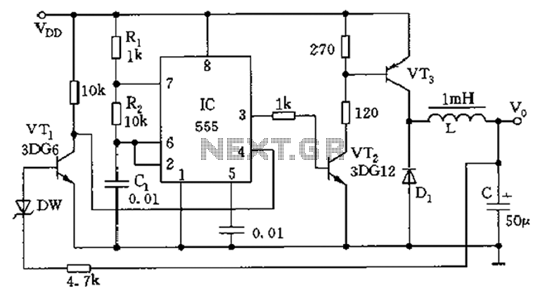
The circuit consists of a 555 timer configured as an astable multivibrator along with resistors R1 and R2 and capacitor C1. It generates an oscillation frequency of approximately 10 kHz with a duty cycle close to 50%. Transistors VT2...
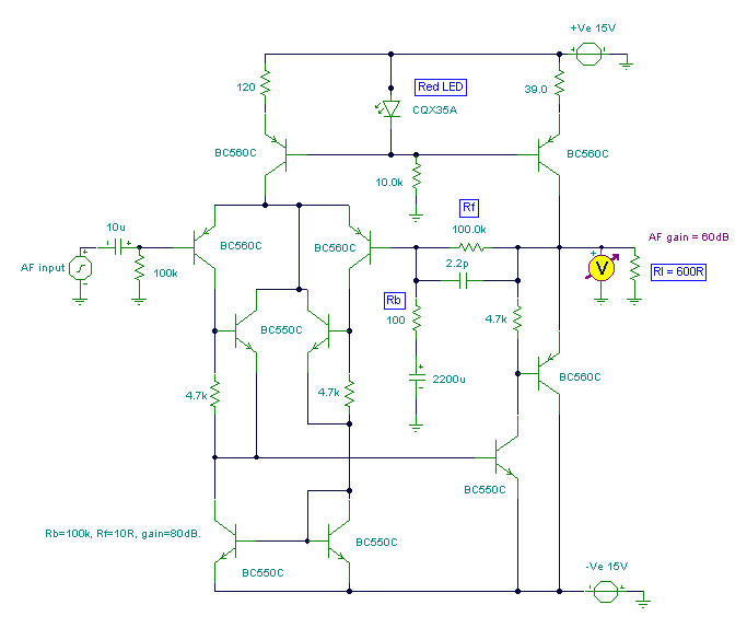
This circuit exhibits an exceptionally fast high-frequency response, as demonstrated by applying a 100 kHz square wave to the input. All graphs were produced using Tina Pro. The circuit's design is optimized for high-frequency applications, showcasing rapid response times that...
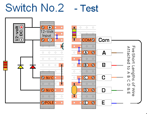
The prototype of Keypad Switch No. 2 was constructed using only the stripboard layout as a reference. If the layout has been accurately reproduced, a functional circuit will result. Once the layout is confirmed to be correct and a...

A simple Hi-Fi amplifier circuit diagram with a schematic for creating an audio amplifier design using the TDA 2616 IC. This is a stereo power amplifier suitable for radio, tape, and television applications, delivering 2 x 12 watts, totaling...
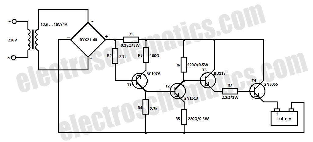
The car battery charging current is automatically limited to 4.2A. If there is a 600mV voltage on R1 (indicating 4A flowing through it), the T1 transistor begins to conduct. This prevents excessive charging current as the base current of...