
Digital Audio Selector Circuit

The circuit design utilizes switched emitter followers to achieve improved performance in signal integrity, particularly in applications where multiple channels operate simultaneously. Switched emitter followers are advantageous due to their ability to provide low output impedance and high linearity, which minimizes signal distortion and enhances the overall fidelity of the circuit.
In this configuration, each channel is isolated from the others, significantly reducing crosstalk, which is critical in multi-channel systems such as audio mixers or communication devices. The specification of handling up to 4 Vms indicates the circuit's robustness and capability to operate effectively within a wide voltage range while maintaining high performance.
The implementation of this circuit may involve transistors configured as emitter followers, where the input signal is fed to the base of the transistor, and the output is taken from the emitter. The switching mechanism can be achieved using control signals that turn the transistors on or off, thus allowing or blocking the signal path. This design choice leads to a more straightforward and reliable operation compared to traditional CMOS switches, which may introduce additional complexities and potential points of failure.
To further enhance performance, careful attention should be paid to the layout and grounding techniques to minimize parasitic capacitance and inductance, which can contribute to crosstalk and signal degradation. Overall, this circuit is well-suited for applications requiring high fidelity and low interference between channels. This circuit, uses switched emitter followers, rather than the usual analog switch CMOS chips. This yields better reduction of crosstalk between channels. This circuit can handle up to 4 Vms with less than -80-dB crosstalk.
Related Circuits

DSP Applications in ADSL (Asymmetric Digital Subscriber Line) can be explored further in Microsoft Office Word. The widespread popularity of the World Wide Web has led to unprecedented levels of Internet traffic. A recent study by the Wall Street...
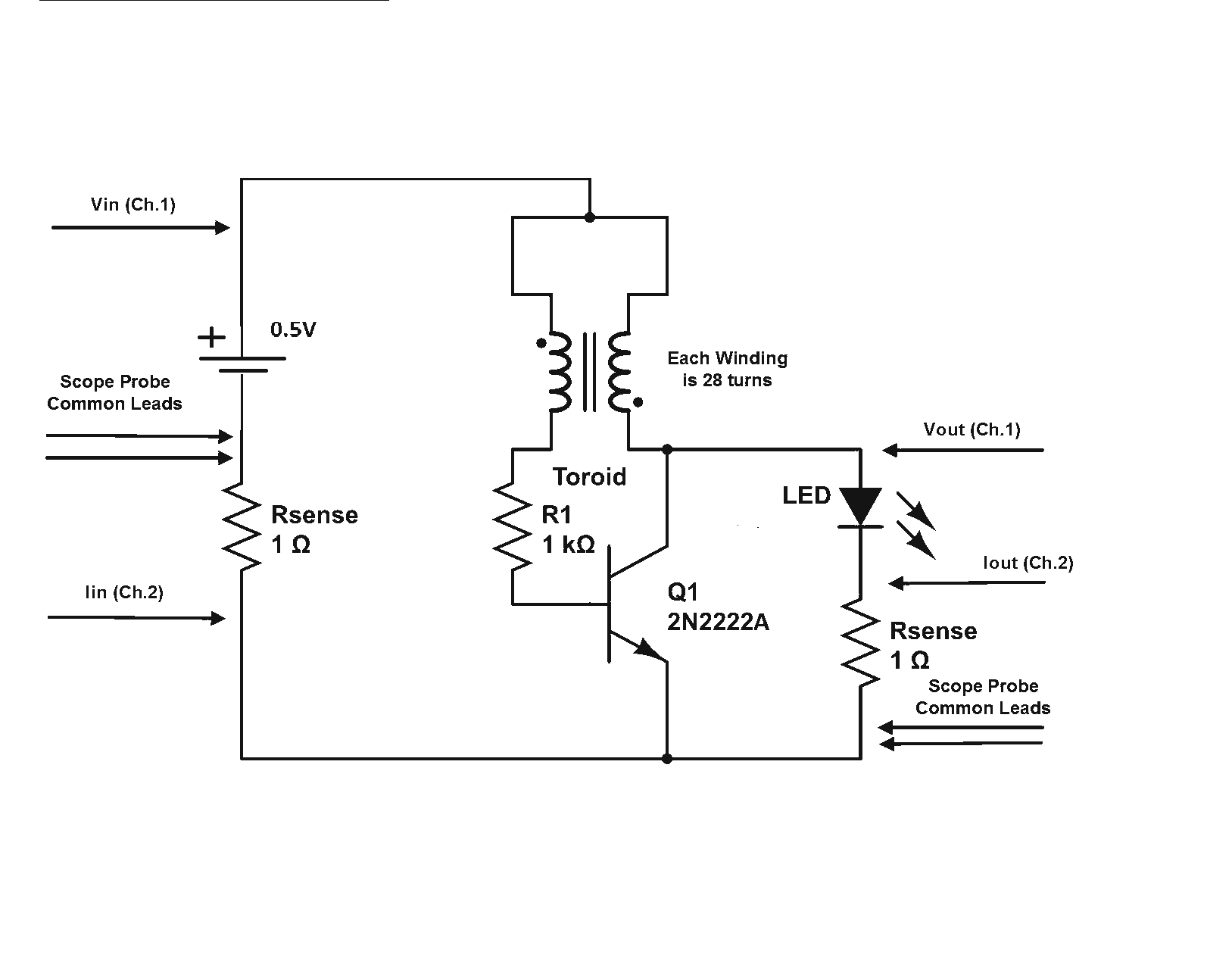
Is a Joule Thief circuit capable of achieving overunity? Joule Thief schematic including scope measurement points. The Joule Thief is a minimalist circuit designed to extract energy from low-voltage sources, such as depleted batteries, and convert it into a usable...
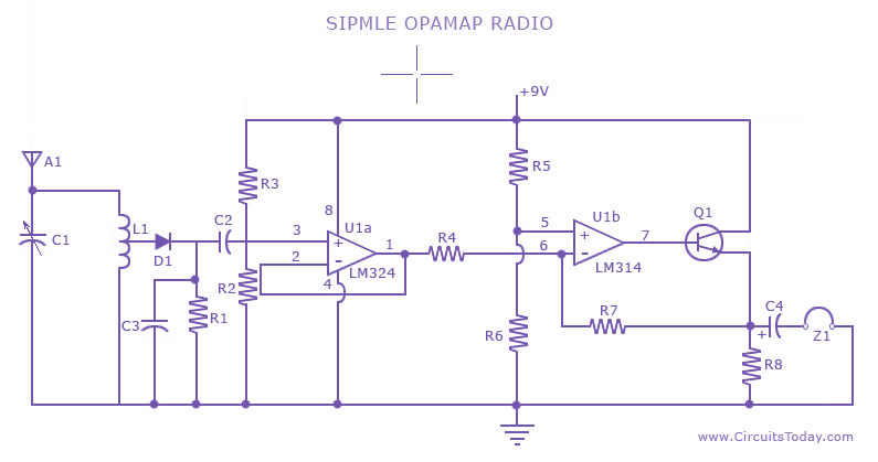
A low-cost, simple radio circuit schematic using an operational amplifier. This radio circuit diagram consists of a sensitive audio amplifier that receives strong signals. The presented radio circuit schematic utilizes an operational amplifier (op-amp) to create a cost-effective and straightforward...
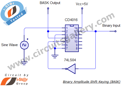
Binary Amplitude Shift Keying (BASK), also known as On-Off Keying (OOK), is a digital modulation technique where the amplitude of the carrier signal is altered according to binary data. This modulation scheme is utilized for transmitting digital information over...
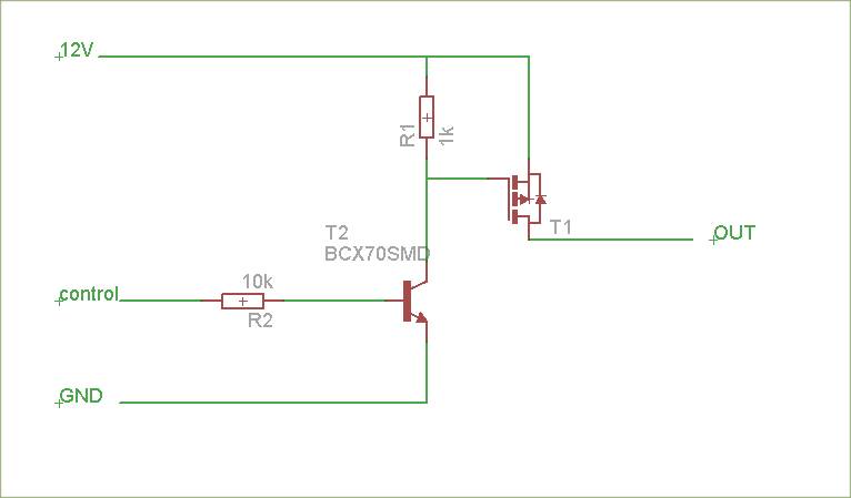
The schematic is attached. Suggestions for improvements are requested, particularly for adding reverse polarity connection protection. The logic level inputs (5 V) are designed to control two output voltages (12 V) using P-channel MOSFETs. The P-channel MOSFETs are ON...
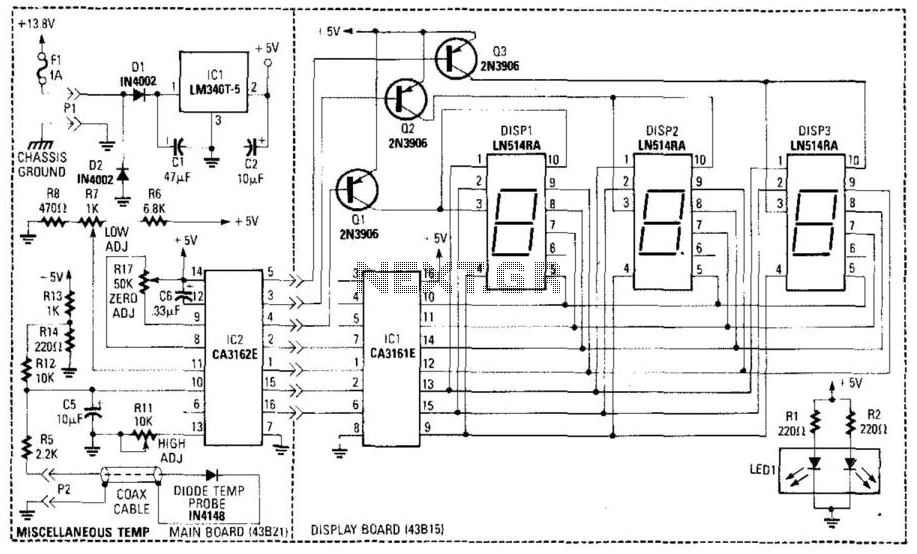
A diode (IN4148) is utilized as a temperature sensor. IC2 is an A/D converter with BCD output. A reference voltage set by R7 is applied to the positive input of IC2. As the temperature rises, the voltage across the...