
Digital Ber-password circuit

The Digital Combination Lock Circuit is designed to provide a secure method for controlling devices through a simple user interface. The LS7220 IC serves as the core component, managing the input from the keypad and processing the combination entries. The relay output allows for versatile applications, enabling the control of various electronic devices such as lights, motors, or alarms based on the user's input.
To implement the circuit, it is essential to ensure proper connections between the IC and the switches. The four switches designated for the combination must be connected to the specified pins, enabling the user to input their unique four-digit code. The additional switches connected to pin 2 act as a safeguard, resetting the system if an incorrect entry is detected, thus enhancing security by preventing unauthorized access.
The timing mechanism, determined by capacitor C1, plays a crucial role in the operation of the relay. The choice of capacitance will directly affect how long the relay remains activated after the correct combination is entered. This feature allows for customization based on the specific requirements of the application, whether for a brief activation or a longer duration.
The layout of the keypad is another critical aspect of the design. Arranging the switches in a 3x4 matrix not only optimizes space on the PCB but also provides a familiar interface for users. The decision to label the keys with symbols instead of numbers can serve as an effective deterrent against unauthorized attempts to gain access, adding an additional layer of complexity for potential intruders.
Overall, the Digital Combination Lock Circuit is an effective solution for implementing electronic access control. Its straightforward design, combined with the flexibility of the LS7220 IC, makes it suitable for a variety of applications requiring secure and reliable operation.Circuit Kunci Digital Ber-password is the circuit diagram of a simple electronic combination lock usingLS 7220. Circuit Kunci Digital Ber-password Password Digital can be used to activate a relay for controlling (on & off) any device when a preset combination of 4 digits are pressed.
The circuit can be operated from 5V to 12V. To set the combinatio n connect the appropriate switches to pin 3, 4, 5 and 6 of the IC through the header. As an example if S1 is connected to pin 3, S2 to pin 4, S3 to pin 5, S4 to pin 6 of the IC, the combination will be 1234. This way we can create any 4 digit combinations. Then connect the rest of the switches to pin 2 of IC. This will cause the IC to reset if any invalid key is pressed, and entire key code has to be re entered.
When the correct key combination is pressed the out put ( relay) will be activated for a preset time determined by the capacitor C1. Here it is set to be 6S. Increase C1 to increase on time. For the key pad, arrange switches in a 3X4 matrix on a PCB. Write the digits on the keys using a marker. Instead of using numbers I wrote some symbols!. The bad guys will be more confused by this. 🔗 External reference
Related Circuits
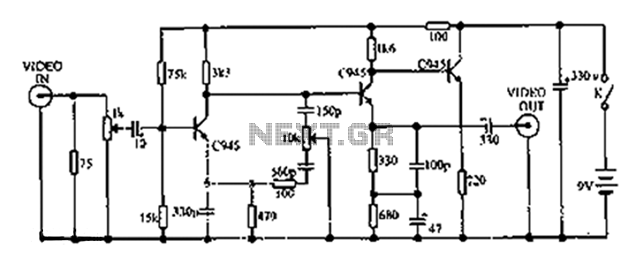
This circuit compensates for additional defects in image quality associated with LP (long play) recorders. The frequency components of the television signal reflect the details displayed on the screen. Enhancing the high-frequency components increases the edge sharpness of the...
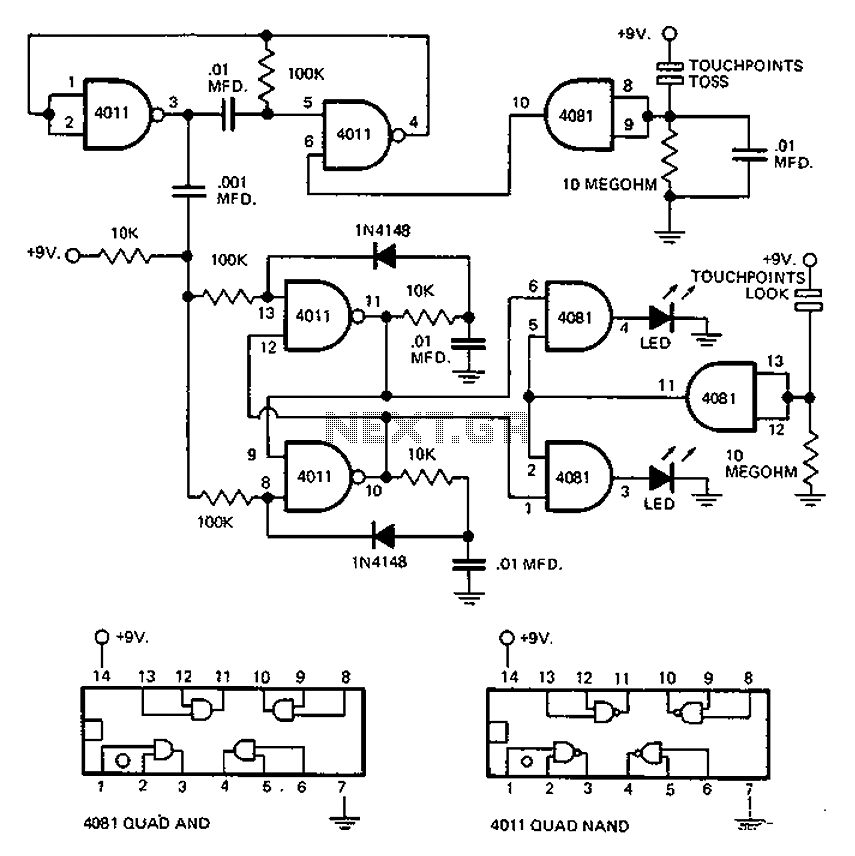
This circuit employs an astable multivibrator to alter the state of a signal based on specific conditions. It also incorporates a flip-flop, which retains the state of the output once a change is detected, completing a cycle of the...

This circuit triggers an alarm when its LDR (Light Dependent Resistor) sensor is exposed to light from the sun or a lamp. A 555 astable multivibrator is utilized to generate a tone of approximately 1 kHz upon detecting light....

Both specifications were contradictory; a large display would require a significant amount of power, while the intention was to use the smallest battery for the longest duration. The solution was to separate the power supply for the logic and...
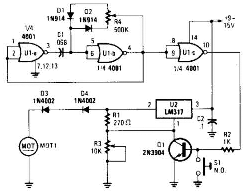
Connected in this manner, an LM317 1-A adjustable-voltage regulator can be utilized to control the speed of a miniature DC motor or to adjust the brightness of a small lamp. The circuit achieves this by modulating the pulse width,...
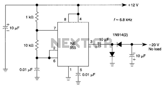
This DC negative-voltage generator based on the 555 produces a negative output voltage equal to approximately 2 times the DC supply voltage. The described circuit utilizes the popular 555 timer IC configured in an astable or monostable mode to generate...