
Digital Camera 5 channel power supply MAX1565

The MAX1565 power supply design for a digital camera is a sophisticated system that addresses the varying power needs of the device. The chip's architecture is built around efficient power management, ensuring that the voltage and current supplied to different components of the camera are stable and within specified limits.
The primary function of the MAX1565 is to generate multiple output voltages from a single input source. This is achieved through the use of pulse-width modulation (PWM), which allows for precise control of the output voltage levels. The PWM signals generated by the DL3 chip are crucial for controlling the external FETs that regulate the power delivered to the camera's various subsystems.
The output stages, which include the rectifier circuits, are designed to convert the PWM signals into smooth DC outputs. The +15V and +7V outputs are particularly important for powering high-demand components such as the image sensor and processing unit, while the additional +V and +1V outputs cater to lower voltage requirements, possibly for auxiliary components or logic circuits.
The implementation of field-effect transistors (FETs) in the switching stages allows for rapid switching and high efficiency, minimizing power loss during operation. The dual PWM circuits provide redundancy and flexibility, enabling the system to adapt to varying load conditions without compromising performance.
Overall, the MAX1565-based power supply design is an exemplary model of modern power management techniques, showcasing the integration of advanced semiconductor technology to meet the demanding requirements of digital camera systems.Digital Camera 5 channel power supply MAX1565 5 shows a digital camera power supply channel MAX1565, seen from the figure, the chip offers a number of road width signal generat ion and control circuit, using different ways according to the DC voltage regulator and current required for the digital camera. DL3 chip 71-pin output voltage type PWM drive signal - external FET work in the off state, the switch transformer primary winding Tl formed PWM pulse current through the switch becomes secondary voltage multiplier Tl Road rectifier outputs respectively +15 voltage V (20 mA) and 7.V (20 rnA) of.
DL1, DL2 output terminal liter pressure type PWM signal, respectively, by the FET switch and rectifier filter circuit +V and +1V output voltage. There are two PWM circuit, a set of switches via respective field effect transistor, the DC voltage into a switching pulse.
Then via the filter circuit output DC voltage to the CPU and other circuits.
Related Circuits
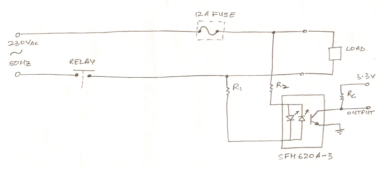
The circuit utilizes an optocoupler (MOC3021) to detect the On/Off state of an electrical appliance using a microcontroller (ATmega16L). The mains supply specifications are 230V, 50Hz. The design aims to determine whether the load is active or inactive. The...
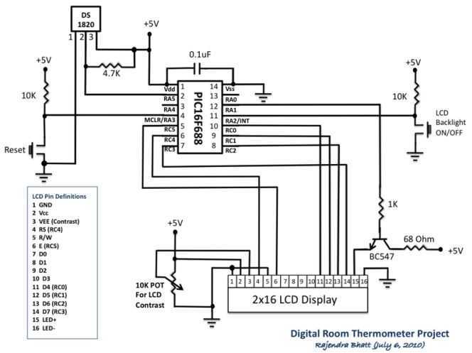
Room temperature plays a vital role in determining human thermal comfort. This digital thermometer is designed to measure room temperature and display it on a LCD screen in both Celsius and Fahrenheit scales. A PIC16F688 microchip is used as...
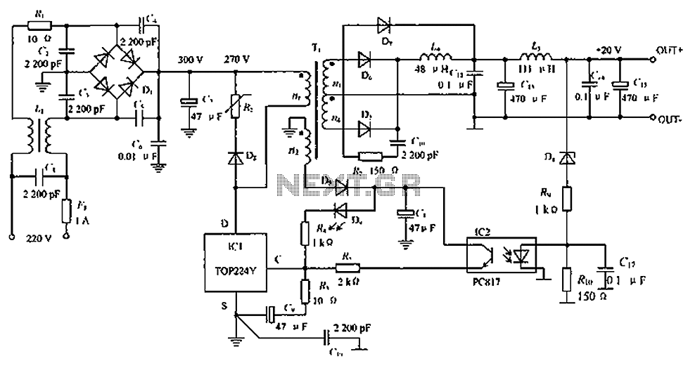
The circuit depicted in the figure is designed to achieve a higher power output by modifying specific components. On the left side of the figure, components R1, L1, D1, and capacitors C1 to C7 form a conventional filtering and...

This high-performance video camera link transmits signals from a video camera to a VCR or from a VCR to TVs throughout a home. The initial stage of the RF chain features a crystal-controlled oscillator, Q1, operating at a frequency...

New cellular phones have incorporated high-resolution cameras that require bright illumination of the surrounding area to achieve high-quality pictures. Traditional xenon-filled photo flashes cannot be used due to the limited space available in cellular phone cameras. Instead, design engineers...
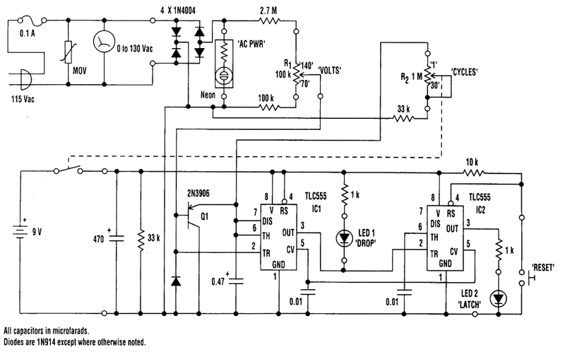
The 0 to 130-volt voltmeter and neon "AC PWR" lamp provide an average indication of AC power. The fuse and metal oxide varistor (MOV) protect the monitor against overvoltage spikes. Four 1N4004 diodes rectify the AC voltage, generating negative-going...