
Digital circuit touch delay circuit 3

The CD4069 integrated circuit is designed for applications requiring a delayed response to a touch input, effectively functioning as a capacitive touch switch. The circuit's operation begins with the capacitive coupling of the user's finger to the input of inverter I. The induced signal creates a condition where the inverter's output switches from a low to a high state, triggering a sequence of events that results in the activation of the connected load, typically a light source.
The charging of capacitor C through diode VD1 is crucial for establishing the delay mechanism. The time constant of the circuit, determined by the resistor R and capacitor C, dictates how long the output remains high after the initial touch. This delay allows for a smoother transition and prevents accidental activation due to transient signals.
The thyristor VT1 plays a vital role in controlling the light output. Once triggered by the high output from the inverter, VT1 remains in a conductive state until the input signal is removed, allowing the light to stay on for a predetermined duration. The design ensures that the circuit can handle a variety of loads, making it versatile for different lighting applications.
In addition to its primary function, the CD4069 circuit can be enhanced with an LED indicator to provide visual feedback on the switch's status. This feature is particularly useful in low-light environments, ensuring the user can easily identify the switch's position.
The configuration of the inverters within the CD4069 allows for flexibility in circuit design. While two inverters are utilized for the touch sensing function, the remaining inverters can be employed for other logic operations or connected to ground, maintaining circuit integrity and reducing the risk of interference.
Overall, the CD4069 integrated circuit represents a robust solution for touch-based switching applications, combining simplicity, efficiency, and reliability in its design. CD4069 is a digital integrated circuit fabrication using boron to delay light touch, it also uses j -wire connection force method, it can directly replace ordinary light switch , without having to change the original interior wiring. When a finger touches M, the body induced by the clutter signal is applied to the inverter I destroyed the input side, so that inverter j is inverted output becomes o, capacitance c. (F .1F negative) on the adoption of VD1 charge. inverter outputs a high level l, the well through R, Since the charge e. This will make subsequent stage VT1 etc. thyristor switch circuit is turned slightly lag time some Furthermore VT1 conduction DC Tian Yong will make the drop F c, charging less influence extended delay time.
By R;, c. A short delay, the output of the inverter t high level 1, Yi R. Trigger VT1 conduction, bidirectional thyristor VTH products also will be turned on, lights point F light. After manpower away from the electrode sheet M, inverters I jump into a high level 1, VD1 is turned off, the capacitor C is discharged through the discharge end of the resistor R, the inverter output low., Complex circuit with sword original state, the thyristor VT1, VTH are switched off F [l E quenching lamp off.
LED night light can be used to switch position indication, for convenience. Feng asked to delay circuit when the R, (1, ask constant discharge decision, Tao Qin little data about imin the right. The electricity is characterized by a hoof products, VT1 Cambodian drive power by a small one-way thyristor product waist thyristor VTH.
because while larger load power circuits, and can drive oOOW ooow less electricity load, 4 ten inverters I ~ IV is available a 6-CD4069 inverter number electrical hoof, in the manifold the other two inverters hemp without its input terminal for grounding, and may not vacant, since [0 Furthermore easy to disrupt the normal circuit [for.
Related Circuits

There are several methods to input a signal into the NE602. Simple untuned approaches (a and b) are viable. For tuning to a specific frequency, an LC resonant circuit with ungrounded trimmer capacitors (c and d) or grounded variable...
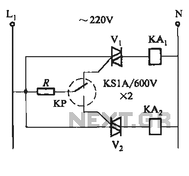
To prevent the failure of electric contact pressure thermometer contacts due to singeing, it is advisable to enhance the contacts, as illustrated in Fig. 11-60. Specifically, the output termination table for DC control utilizes two two-way thyristors or a...
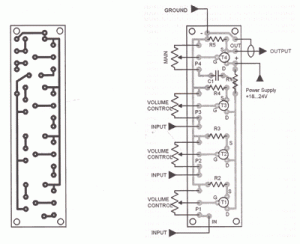
This FET audio mixer demonstrates the versatility of FETs. Originally designed for high-frequency applications, FETs can also effectively handle audio frequencies, showcasing exceptional performance in this domain. The circuit can accommodate an unlimited number of inputs, provided that the...
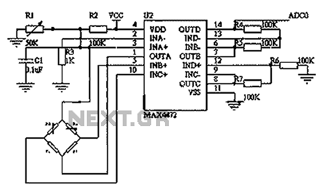
This circuit utilizes a BP01-type pressure sensor and the MAX4472 operational amplifier. The BP01 pressure sensor is specifically designed for blood pressure detection and is primarily used in portable electronic sphygmomanometers. It features a precision thick film ceramic chip...
The goal is to transmit additional information through the use of articles. If there are any issues related to article content, copyright, or other concerns, please contact us via email at [email protected] within 15 days. The content will be...
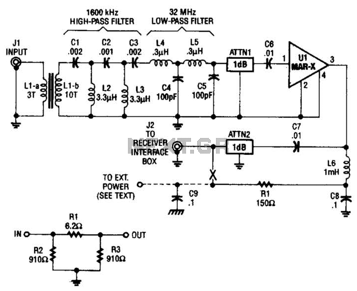
The HF/SW receiver preamplifier consists of a broadband toroidal transformer (LI-a and Ll-b), an LC network featuring a 1600-kHz high-pass filter and a 32-MHz low-pass filter, inductors L2 and L3 (26 turns of #26 enameled wire wound on an...