
digital clock

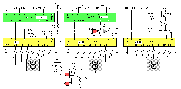
The digital clock circuit utilizes a combination of integrated circuits to manage timekeeping and display functions. The primary components include a microcontroller or timer IC, which serves as the core of the clock, along with additional ICs that handle the display and power management. The use of two distinct voltage lines, +5VA and +5VB, is crucial for the operation of this circuit. The +5VA line ensures that the majority of the circuit components are powered, while the +5VB line is specifically designated for the display and certain ICs, allowing for efficient power management.
In the event of a power failure, the circuit is designed to switch to battery operation, maintaining timekeeping functionality. This is achieved through a carefully designed power management system that disconnects the display from the main power supply while keeping the microcontroller operational. The incorporation of this feature is essential for ensuring that the clock remains functional even during power outages, thereby enhancing its reliability.
For PCB fabrication, the process begins with designing the layout in software such as Eagle, which provides tools for creating and modifying circuit schematics. Once the design is finalized, it can be printed onto photo or glossy paper using a laser printer, which is critical for achieving a high-quality transfer of the circuit pattern to the PCB. The printed design must then be adhered to the copper side of the PCB, followed by the application of heat using a hot iron. This step is crucial as it allows the ink to bond with the copper, creating a resist for the etching process.
After the design has been transferred, the PCB can be etched using a suitable etching solution, which removes the unprotected copper and leaves behind the desired circuit pattern. Once the etching is complete, the board can be drilled for component placement, and the components can be soldered in place to complete the assembly of the digital clock circuit. This methodical approach ensures that the final product is both functional and reliable, suitable for practical applications in timekeeping.This is digital clock schematic diagram. This circuit is quite complex and quite difficult for a newbie because this circuit uses IC with some a complicated connections. The voltages that supplied to the circuit are divided in two lines. The voltage +5VA supplies all IC except the IC9 until IC13 and is supplied with voltage in case of break of ne
twork voltage. On the other side, the voltage linr of +5VB only supplies the IC9 until IC13 and display and is interrupted in case of interruption of network voltage, it is to ensure the economy of battery. Make a PCB in very easy steps. ! Create your PCB design using PCB designer software like Eagle, print out your design on photo paper or glossy paper with laserjet printer.
Stick the printed design on the PCB (copper side) and then heat it using hot iron plate. The ink will stick on the PCB and it will be ready for etching process. Note: If you don`t have laserjet printer, then you can print the design on standard paper. Copy the printed design at Copy Service around your location (with glossy paper). 🔗 External reference
Related Circuits
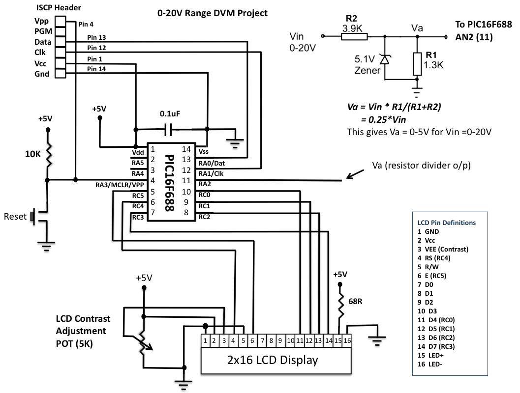
This is another version of an older digital voltmeter (DVM) project that was based on the PIC12F683 microcontroller. The previous version displayed the measured voltage on an LCD driven serially by the PIC12F683 using three I/O pins. The new...
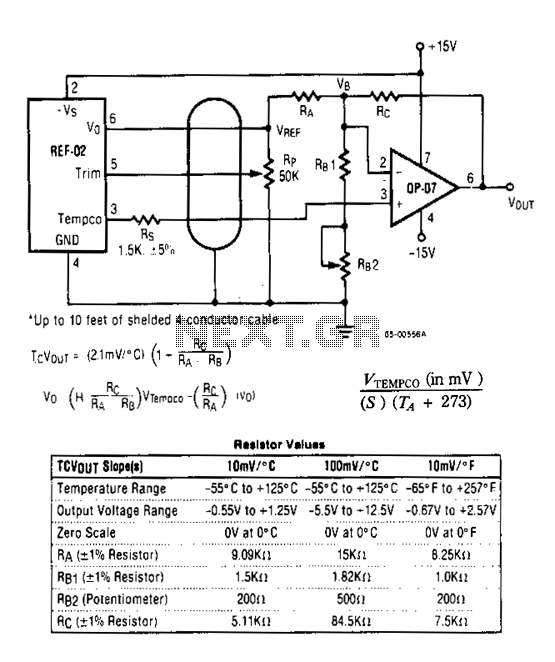
The DVM-to-temperature adapter is constructed around a single integrated circuit (IC), the National LM10. This micropower IC features a stable 0.2 V reference, a reference amplifier, and a general-purpose operational amplifier. The circuit is designed to operate within a...
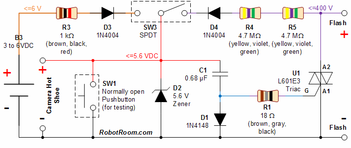
This circuit incorporates a datasheet-compliant trigger signal, reversed polarity protection, an optional test button, and the capability for battery operation. It utilizes either the U1 L601E3 or MAC97A8 triac, rated for 400 V and 1 A. When U1 is...
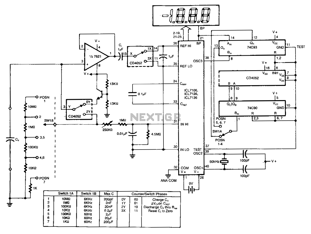
The circuit charges and discharges a capacitor at a crystal-controlled rate and stores the change in voltage achieved on a sample-and-difference amplifier. The current flowing during the discharge cycle is averaged and ratiometrically measured in the analog-to-digital converter (ADC)...
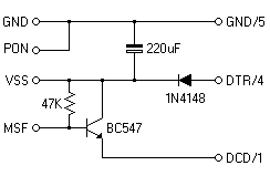
The three best known of these signals are the DCF77 signal broadcast from Mainflingen near Frankfurt in Germany on 77.5kHz which can be received throughout most of central and northern Europe. The MSF signal broadcast from outside Rugby in...
This device is a combination digital clock timer and solar panel charge controller designed to maintain a deep cycle battery charged by a solar panel. The timer output controls a 12-volt load for a 32-minute interval each day. The...