
Digital thermometer circuit based on CA3162 CA3162 and LM35

The digital thermometer circuit described is designed to provide an accurate and efficient means of measuring temperature without the complexity of a microcontroller. The integration of the CA3162 A/D converter allows for precise conversion of the analog voltage from the LM35 temperature sensor into a digital format suitable for display. The dual slope A/D conversion method enhances measurement accuracy by averaging out noise and fluctuations in the input signal.
The CA3161 serves as an effective interface between the digital output from the CA3162 and the visual representation on the seven-segment display. By eliminating the need for additional current-limiting resistors, the CA3161 simplifies the circuit design and reduces component count, contributing to a more compact and efficient layout.
The use of potentiometers for gain and zero adjustments provides flexibility in calibrating the thermometer for different applications or environmental conditions. Additionally, the ability to switch between low-speed and high-speed modes allows the user to tailor the sampling rate according to the specific requirements of the measurement task, whether prioritizing power consumption or response time.
Overall, this digital thermometer circuit exemplifies a practical application of integrated circuit technology in temperature measurement, showcasing the synergy between analog sensing, digital processing, and user-friendly display.A simple digital thermometer circuit with out a micro controller and having a seven segment LED read out is shown here. The circuit is based on three ICs: CA3162, CA3161 and LM35. CA3162 is a monolithic analogue to digital (A/D) converter that has BCD output. The A/D converter inside the IC is a dual slope type with differential inputs. The IC has an internal timing circuitry and hold function. When the hold function is enables, the output IC latches itself to the present state. CA3161 is a monolithic BCD to seven segment converter IC. It can directly drive a seven segment display and there is no need for current limiting resistors. LM35 is a three terminal precision temperature sensor IC from National semiconductors. The output of LM35 is highly linear and has a scale factor of 10mV/C. The IC consumes only 60uA as standby current and is calibrated directly in degreeCelsius. IC LM35 is used for sensing the temperatures. A voltage proportional to the temperature will be available at pin 2 of the LM35 and this voltage is coupled to the high input pin (pin11) of the CA3162. CA3162 does the job of converting this analogue voltage in to a BCD format. POT R1 connected at pin 13 of the CA3162 is used for gain adjustment while POT R2 can be used for ZERO adjustment.
Capacitor C2 is the integrating capacitor of the A/D converter circuitry inside the IC. The working of the CA3162 is as follows, the voltage applied to the input pin (pin11) is converted into a current (using the built in V/I converter circuit) that charges the integrating capacitor C2 for a preset amount of them. Then the integrating is disconnected from the V/I converter circuit and a reference constant current source is connected to the integrating capacitor.
The time taken for the charge to restore to its original value is noted and the number of clock cycles elapsed during this time will be a measure of the charge induced by the input voltage (voltage applied to pin 11). The point of restoration is sensed using an internal comparator which latches the counter and the count is then multiplexed into the BCD outputs and the entire cycle is repeated.
The hold pin CA3162 (pin6) can be used for running the IC in different modes. When the hold pin is grounded or left open the IC runs in low speed mode (sampling rate is 4Hz). When hold pin is held at +5V, the IC runs in high speed mode i. e. a sampling rate of 96Hz. When the hold pin is held at a fixed 1. 2V, the BCD output latches to the current state. C1 is the power supply bypass capacitor whose job is to bypass noise if any from the power supply line. The next section of the circuit is the BCD to seven segment decoder plus display driver section. For that purpose CA3161 is used. The BCD output pins of the CA3162 are connected to the input pins of the CA3161. Transistors Q1, Q2, Q3 common anode terminals of the corresponding seven segments displays. Q1, Q2, Q3 are driven by the 4, 3, 5 pins (digit driver pins) of the CA3162 respectively. 🔗 External reference
Related Circuits
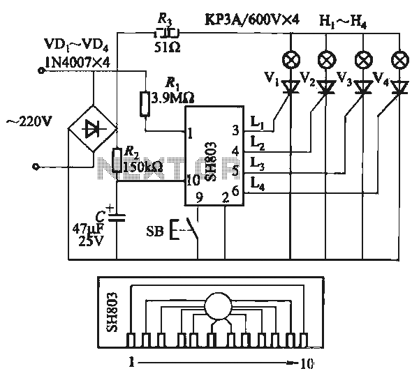
The circuit utilizes the SH803 flash IC, which can store eight different programs and offers various dimming options and light speed adjustments. A button is provided to trigger the control terminal SB on the 9-pin connector for program selection,...
Analog-to-digital converters (ADCs), printed-circuit board (PCB), microcontroller or digital signal processor (DSP), total-harmonic-distortion (THD), signal-to-noise ratio (SNR). Analog-to-digital converters (ADCs) are essential components in modern electronic systems, enabling the conversion of analog signals into digital form for processing by microcontrollers...
A voltage divider is created using resistors R2 (10MΩ) and R3 (100KΩ), which effectively reduces the voltage across capacitor C2 by a factor of approximately 100. The ground of C2 is connected to the inverter ground for reference. An...
The circuit illustrated in the schematic diagram below allows for the visualization of the direction and shaft rotation of a stepper motor on an LED display. Instead of employing a digital rotation encoder as an input, this circuit utilizes...
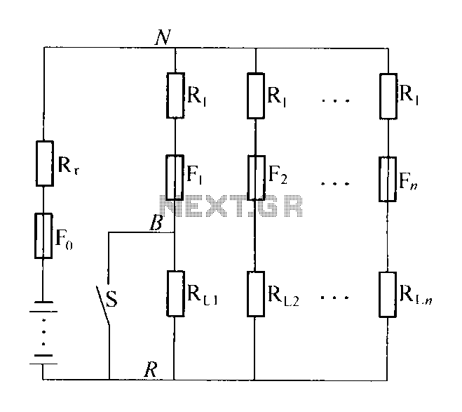
The circuit diagram illustrates a high-impedance distribution system characterized by low resistivity distribution. A notable feature is the series resistance of the shunt load current limiting resistor R1, typically valued at five to ten times the internal resistance of...
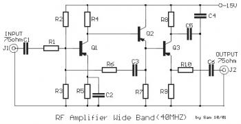
This is a 40 MHz RF amplifier circuit. The sensitivity of a receiver can be significantly enhanced by integrating this circuit between the receiver and the antenna. The amplifier does not utilize resonant circuits and is suitable for both...