
Downlink Project Description

The Skeyeball project integrates several key components and methodologies to facilitate effective data transfer from an aircraft to the ground. The system architecture includes a combination of analog and digital circuitry, with a focus on optimizing bandwidth for data transmission. The analog circuits are responsible for handling the NTSC video signal, ensuring that data is injected and extracted during non-visible periods of the video frame. The use of Xilinx FPGA technology allows for flexibility and scalability in the digital processing of the signals, accommodating future enhancements in data rates and functionality.
The implementation of the MC1489 and MC1488 chips for serial communication ensures reliable data transfer between the airborne and ground systems. The careful design of the analog section on a breadboard enables iterative testing and refinement, which is crucial for achieving the desired performance levels. The integration of the MX045 clock generator facilitates accurate timing for data transmission, while the Xilinx 4010 chip's capability to process sync pulses enhances the system's efficiency in data handling.
Overall, the Skeyeball project exemplifies a comprehensive approach to embedded system design, combining theoretical knowledge with practical application to achieve a functional and efficient data downlink system. This project not only serves educational purposes for students involved but also contributes to advancements in embedded systems and RF communication technologies.The Skeyeball project is an ongoing project in the Indiana University System Design Methods Laboratory for both graduate and undergraduate students to perform embedded system design and implement various projects. The downlink portion of the project involves transfering data from the plane to the ground by using a single signal.
My downlink p roject involves re-implementing Prashant Patel`s project from thesummer of 2000, then compacting and debugging it to achieve the desired operation. The first step is to implement the xilinx code using two Logic Engine Boards to host the plane and ground implementation seperately so that adequate testing with the RF transmitter and receiver can be accomplished.
I also re-implemented the analog injection and extraction ciruits with new designs to increase bandwidth. A NTSC signal is generated by the video source and it`s horizontal and vertical synchronizing pulses allow data to be injected at spaces in the signal where the video signal is retracing to the top of the screen and is always black.
The data can be injected in these spots and then extracted from the same spot by the same manner. Once the data is extracted, the video signal is set back to black so that there are no side effects in the video image displayed on the monitor. There are 10 of these spaces in each field and a maximum bandwidth of 300 bits per space. The present goal is an established 56kbps downlink, which is around 90 bits per space. The limitation to higher bps is the bandwidth the RF transmitter, receiver and the analog circuitry allows.
Maximum bps is determined experimentally. The data is viewed using hyperterminal, so a lower rate is better. Once further parts of the system are operating we can increase the download capabilities. The physical part of the project has to be done in two phases the testing phase and the finished project. When fin ished the injection circuitry will be added into the fusilage of the plane, and the extraction circuitry will be o n the ground.
This diagram illustrates how the fit in to the bigger picture. The injection circuitry will communicate with the tracking component via a serial link. It is currently setup to recieve at 9600bps, which can be increased in the future. The transmitter and receiver are dealing with the video signal which has the data in it. On the ground side, after the data is extracted, it can be displayed through hyperterminal, or any other serial interface. and the video can be observed on a monitor. For the testing phase I setup the equipment on two Logic Engines. These provided a good foundation to work off of because the have the structure to do wire wrapping and the slots for the neccesary pins.
I used the MC1489 and MC1488 chips on the board to send out and recieve the serial communication since they are wired to the serial cables. The analog portion was designed by Bryce Himebaugh and implemented on a bread board with individual resistors, capacitors, and transistors, so that refinements could easily be made on it.
After a few changes to the resistance and capacitance, the analog portion was behaving as expected. This portion is given the video signal and then using a signal synch separator sends the vertical and horizontal synch pulses to the digital portion, it then receives the data back during the correct pulses in the vertical retrace. The digital portion is implemented on the Xilinx 4010 chip. This chip allows ample room for the design, as well as plenty of pins for design usage and testing. The clock is provided by the MX045 chip which gives a 20 MHz pulse which is then divided down to produce the desired data pulse rate.
The design takes as input the vertical and horizontal synch pulses from the analog portion of the design. It counts these pulses in order to know when to output the data in the correct spaces. I followed closely to the same design from previous project, and I used macro 🔗 External reference
Related Circuits
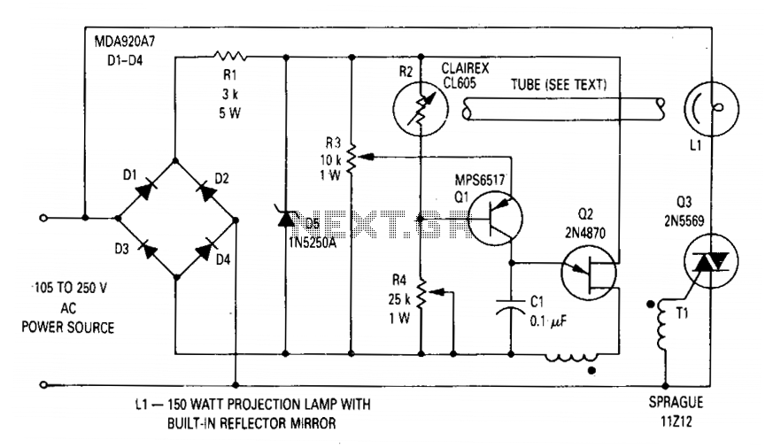
The circuit regulates the RMS output voltage across a load, specifically a projection lamp, to 100 volts ±2% for input voltages ranging from 105 to 250 volts AC. This regulation is achieved by indirectly sensing the light output of...
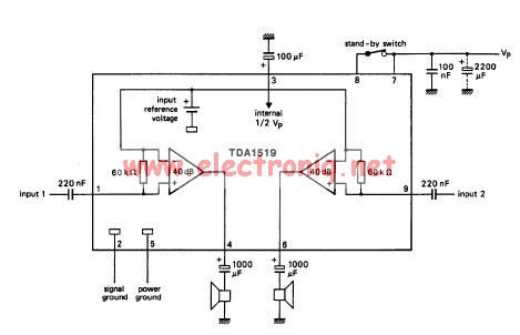
The TDA1519 circuit can deliver 2x6 watts of output power. The TDA1519 is an integrated class-B dual output amplifier housed in a 9-lead single in-line (SIL) plastic medium power package, primarily developed for car radio applications. The TDA1519 amplifier is...
It is possible to control home and office electrical appliances using a mobile phone. This document presents a simple home automation electronic mini project circuit diagram designed for engineering students, allowing the control of electrical appliances without the use...

This volume controller equalizer electronic project is designed using the LM1036 DC tone volume controller, featuring a volume and balance circuit for stereo applications. The four control inputs of the LM1036 volume controller enable the control of bass, treble,...
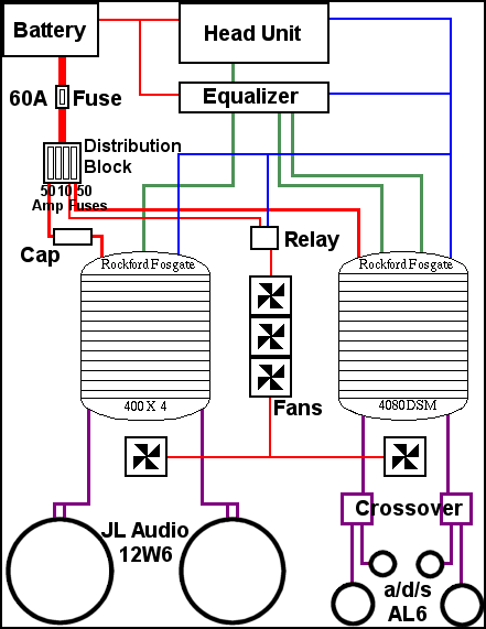
The following circuit illustrates an Electric Car Audio Project. Features include a Rockford Fosgate Punch 4080DSM amplifier, which operates in a bridged 2-channel configuration at 4 ohms for component speakers. The Electric Car Audio Project utilizes the Rockford Fosgate Punch...

H-Bridge circuit utilizing transistors for the bidirectional control of a DC motor. Integrated circuits (ICs) containing H-Bridges are employed to simplify the drive circuit. The L293D is a dual H-Bridge motor driver, allowing for the control of two DC...