
driving a relay
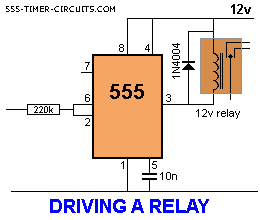
The 555 timer is a versatile integrated circuit widely used in various applications, particularly in timing and pulse generation. In this specific configuration, the 555 timer operates in a bistable mode, where it can toggle the state of the relay based on the input voltage levels at pins 2 and 6.
The circuit design includes a relay that acts as an output device, controlled by the state of the 555 timer. The relay's coil is energized when the output pin (pin 3) of the 555 timer is low, allowing current to flow through the relay, thus activating it. The hysteresis feature is critical in this design, as it provides stability to the circuit by defining two distinct voltage thresholds. The upper threshold (2/3V) ensures that any minor fluctuations in the input signal do not inadvertently trigger the relay, while the lower threshold (1/3V) guarantees that the relay remains inactive when the input is low.
The configuration of the relay can be adjusted depending on the application requirements. If connected in a high configuration, the relay will activate when the output is high, while in a low configuration, it will activate when the output is low. This flexibility allows for various use cases, from simple on/off control to more complex applications requiring precise timing and control.
To enhance the reliability of the circuit, it is advisable to include protection diodes across the relay coil to prevent back EMF from damaging the 555 timer when the relay is deactivated. Additionally, the use of decoupling capacitors near the power supply pins of the 555 timer can help stabilize the voltage supply and further reduce the risk of noise interference.
Overall, this 555 timer relay activation circuit is an effective solution for applications requiring low power consumption and reliable control of relay operations based on input voltage levels.The 555 will activate a relay. When pins 2 and 6 are connected as an input, the chip requires only about 1uA to activate the output. This is equivalent to a gain of about 200, 000, 000 (200 million) and represents about 4 stages of amplification via transistors.
In the first circuit, the output will be opposite to the input. The relay can be connecte d "high" or "low" as show in the second diagram. One point to note: The input must be higher than 2/3V for the output to be low and below 1/3V for the output to be high. This is called HYSTERESIS and prevents any noise on the input creating "relay chatter. " In the first diagram above, the relay is connected so that it is active when the output is low. This is called NEGATIVE or NEGATIVE LOGIC. It has the same reasoning as-5 - (-5) = 0. When the input is low in the first diagram, the output is HIGH and the relay is OFF. The circuitry creates two reversals and makes it easy to see that when the input is LOW, the relay is OFF.
🔗 External reference
Related Circuits
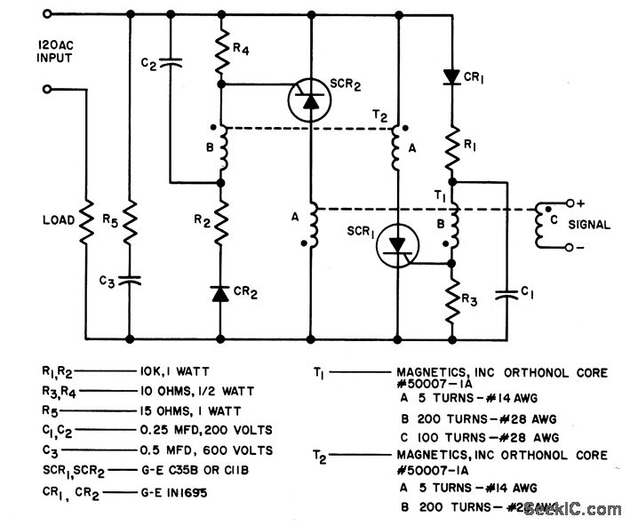
To fulfill the requirements of a control loop, it is often necessary to utilize an electromagnetic relay or a transistor relay to either accelerate or delay an action, thereby forming an acceleration or delay circuit. The circuit depicted in...
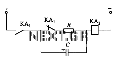
This component is equivalent to a single-pole electromechanical latching relay with an electrically isolated solenoid. Once activated, the circuit remains in a conductive state even if the line voltage is interrupted for extended periods. A positive reset action necessitates...
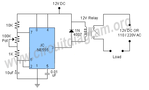
In this circuit, the 555 Timer IC is configured as an astable multivibrator, and a 12-volt relay is operated through pin 3 of the IC. The IC generates continuous pulses at pin 3, which activate and deactivate the relay,...
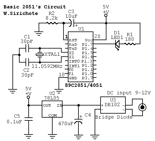
A basic circuit of the 89C2051 can be constructed using point-to-point soldering on a universal printed circuit board (PCB). An ordinary 20-pin socket should be utilized, avoiding the use of a circular-pin socket. D1 represents a small dot LED....
The circuit can also be triggered by logic ICs (TTL/CMOS) using the appropriate interfacing method. Another relay is typically used to serve as the trigger button when interfacing ICs with the latching relay circuit. The described circuit utilizes a latching...
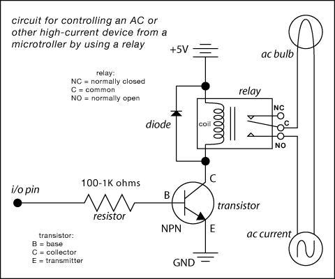
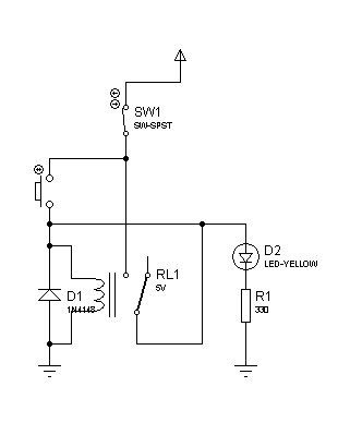
Here are some circuit diagrams for driving relays from a microcontroller. Ensure the use of a 5-volt relay (this refers to the coil, not the load circuit) and verify that the relay has a sufficient rating for the load...