
Dual AC radio remote control switch circuit diagram

The dual radio remote control switch circuit operates effectively by utilizing a combination of oscillators and demodulators to manage multiple frequencies. The transmitter section is designed to generate distinct frequencies based on the switch pressed, allowing for versatile control options. The use of Q3 for high-frequency signal generation ensures reliable transmission over a distance, while the oscillator configuration with Q1 and Q2 enables quick frequency shifts between 5 kHz and 3.7 kHz.
The receiving section is critical for interpreting the transmitted signals. The demodulation process, facilitated by Q4 and Q5, ensures that the audio signals are accurately translated back into control pulses for the bistable circuits. The integration of IC1 and IC2 allows for simultaneous control of two distinct functions, enhancing the circuit’s functionality. The STA401A component plays a pivotal role as it manages the state of the output based on the received pulses, effectively controlling the load and enabling relay operations.
The TLP3503 optical coupling circuit serves as an interface between the low-power control signals and the higher power load, ensuring isolation and protecting sensitive components from voltage spikes. This design choice enhances the reliability and safety of the circuit during operation. The overall architecture of the dual radio remote control switch circuit exemplifies efficient design practices in remote control applications, providing both functionality and ease of use. As shown in FIG AC is a dual radio remote control switch circuit. Transmitter: Q3 generates a high frequency carrier signal. Q1, Q2 composition oscillator circuit. When you pre ss SW1, the oscillation frequency of 5kHz, press SW2, the oscillation frequency is 3.7kHz. When the start-up circuit, LED as work instructions. Receiving circuit: Q4 and peripheral components receiving circuit, two demodulated audio signals, in pre-release Q5, and then into IC1, IC2 of 3 feet. IC1 demodulation frequency 5kHz, the corresponding transmitter SW1, IC2 correspond SW2.SW1 when pressed, IC1 8-pin switch sends a pulse when SW2 is pressed, IC2 pin 8 also sends switch pulses.
Two pulses are fed STA401A. STA401A and peripheral components of two separate bistable circuit. IC1 fed pulse to 4 feet STA401A goes low, TLP3503 (optical coupling circuit) input of a current flowing through the load electrical work. STA401A another way to control relay. Press the appropriate button, STA401A corresponding circuit reset.
Related Circuits
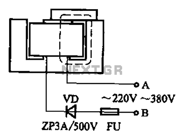
After some minor loss of field magnets, they can be re-magnetized using a homemade method. A scrap of exchanges and contacts, as well as other models like CJ10-60 ~ 15, can be utilized. The circuit operates at 0A (compatible...
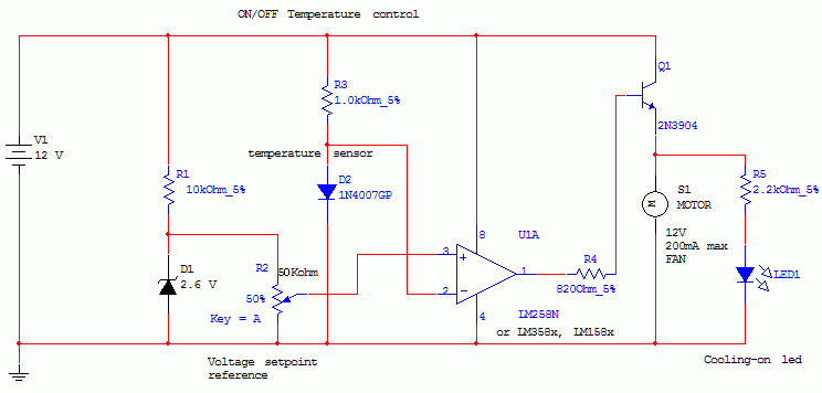
This circuit controls a load, specifically a DC brushless fan, based on temperature compared to a setpoint. The transducer used is a diode operating in the forward polarization regime. When forward-biased, the forward voltage drop across the diode exhibits...
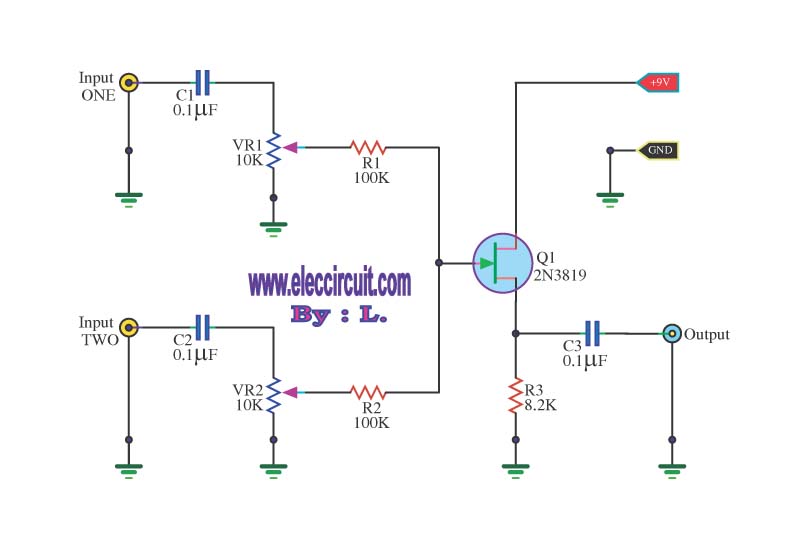
This circuit is a simple mixer circuit that can mix two signal channels into one output channel. It utilizes a codec circuit to convert stereo audio to mono audio. The main component in this circuit is a FET, specifically...

This circuit is a simple mixer circuit that can mix two signal channels into one output channel. It utilizes a codec circuit to convert stereo audio into mono audio. The circuit can also increase the number of channels by...

The electric shaver circuit is illustrated in Figure 1-17. It features a buck capacitor (C) rated at 1 µF and 450V, which connects through diode VD to charge 1.2V nickel-cadmium batteries. Additionally, after the buck converter, there is a...
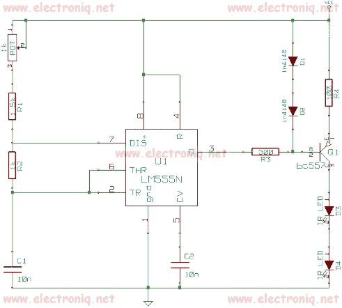
This Remote control Jammer device is useful when blocking someone from using the remote control (such as children who frequently change the channels on the TV). This remote control jammer is very simple and uses two infrared LEDs that...