
Dual Relay Driver Board Circuit

This relay driver circuit is designed to facilitate the control of relays in various electronic applications, making it an essential component in automation and control systems. The BC547 NPN transistors Q1 and Q2 are crucial for amplifying the control signal, allowing for the activation of relays that require a higher current than the control signal can provide. The common-emitter configuration of these transistors not only increases sensitivity but also enhances the overall performance of the relay driver.
The resistors R3 and R4 play a vital role in protecting the transistors from excessive input current, which could lead to thermal runaway or damage. By carefully selecting the resistor values based on the input voltage and desired current levels, the circuit can be optimized for different applications while maintaining reliability.
Diodes D3 and D4 are placed in parallel with the relay coils to handle back electromotive force (EMF) generated when the relay is turned off. This EMF can produce voltage spikes that may damage the driving circuit components. The inclusion of these diodes ensures that such spikes are safely dissipated, enhancing the longevity and stability of the entire circuit.
Overall, this relay driver circuit is a robust solution for interfacing relays in various electronic projects, providing a reliable means of controlling higher power loads while ensuring the protection of sensitive components.A simple and convenient way to interface 2 relays for switching application in your project. This relay driver boosts the input impedance with a regular BC547 NPN transistor (or equivalent). Very common driver. It can drive a variety of relays, including a reed-relay. Transistor Q1and Q2 are a simple common-emitter amplifier that increases the effective sensitivity of the 12 volt relay coil about a 100 times, or in other words, the current gain for this circuit is 100. Using this setup reduces the relay sensitivity to a few volts. R3 and R4 restricts the input current to Q1 and Q2 to a safe limit. Diodes D3 and D4 are EMF dampers and filter off any sparking when the relay de-energizes.. 🔗 External reference
Related Circuits
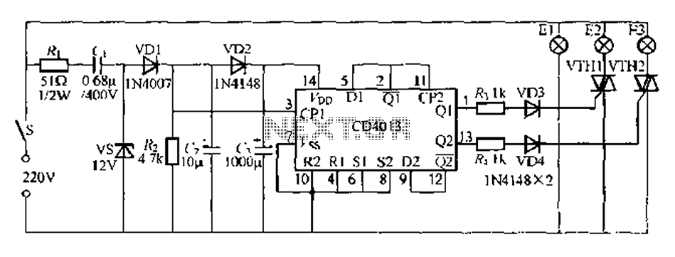
Figure 296 illustrates a control circuit that utilizes a switch (S) to manage three lamps (E1, E2, and E3) in a lighting system, suitable for controlling a chandelier in a living room. When the switch is off, all lights...
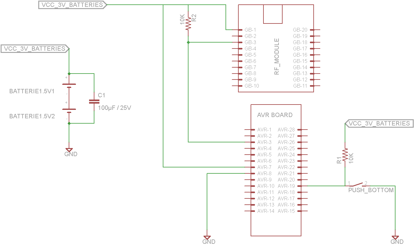
This tutorial demonstrates concepts for creating a lamp with dual actuation. The lamp can be controlled through a parallel switch or by a relay that is managed using an RF module based on the ZigBee protocol (IEEE 802.15.4). The...

The circuit depicted is designed to protect a system from power supplies that may exceed safe limits. An example of this is small consumer products that utilize external AC adapters, where there is a risk of accidentally connecting the...
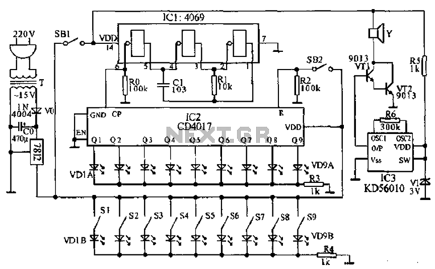
This document presents a principle circuit for electronic games. The main circuit operates in conjunction with the host through the reset button SB2, while the indicators VD1A-VD9A remain off. Prizes, for example, five, are determined by the number of...
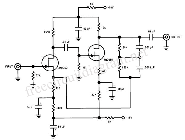
The preamplifier circuit is designed to offer appropriate loading for phono cartridges with reluctance. It achieves a gain of approximately 25 dB at 1 kHz (converting an input of 2.2 mV to an output of 100 mV). The circuit...
The delay application circuit is depicted in Figure JEC-2, which consists of two components. When the input transitions from logic level 0 to 1, the output also changes to 1 immediately. However, when the input transitions from high level...