
JEC-2 delay circuit diagram consisting of b

The delay application circuit described utilizes a simple RC (resistor-capacitor) network to create a time delay in signal processing. In this configuration, the capacitor charges through the resistor when a high logic level is applied at the input. The time constant of the circuit, which dictates the delay, is defined by the product of the resistance (R) and capacitance (C) values (τ = R × C).
When the input signal transitions from a low state (0) to a high state (1), the output reflects this change immediately. Conversely, when the input signal transitions from a high state (1) to a low state (0), the capacitor discharges through the resistor, and the output remains high until the capacitor voltage drops below a certain threshold. This threshold is determined by the specific trigger level set within the circuit, which can be adjusted to fine-tune the response time of the output.
The circuit is designed to accommodate a broad range of delay times, from as short as 0.02 seconds to as long as 10 seconds. By selecting appropriate resistor and capacitor values, the time constant can be modified, allowing for precise control over the delay duration. For applications requiring shorter delays, decreasing the resistance or capacitance will result in a quicker response. Conversely, increasing either component will extend the delay period.
Furthermore, the circuit can be calibrated to correct any discrepancies in timing by adjusting the resistor and capacitor values. This flexibility makes the delay application circuit suitable for various electronic applications where timing control is critical, such as in signal processing, automation systems, and timing circuits.Delay application circuit is shown in Figure purposes JEC-2 consisting of two. When the input end is logic 0 to 1, the output also immediately end 1 ; but when the input end is high level 1 transition to low level 0, the output by the delay after it becomes 0, the delay time from 10 F capacitor charging to the trigger level to ask the decision. This circuit provides the delay time is 0.02 to 10 seconds, for the case where the delay time shorter.
Change R and C, you can change the delay time. Re value adjustment, you can correct errors.
Related Circuits

This is a multifunction RJ45 network cable tester designed for testing network cables (RJ45) and telephone cables (RJ11). It is cost-effective and user-friendly. The tester determines whether a network cable is a crossover or straight type by illuminating a...
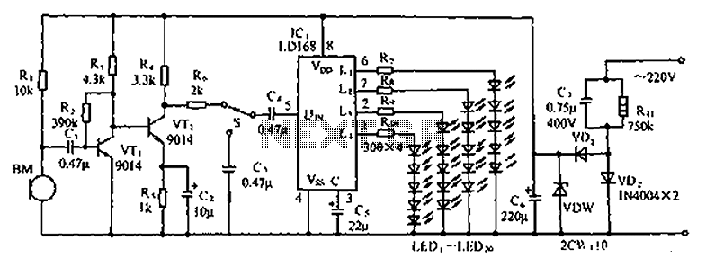
The circuit depicted in the figure involves the LD168, which functions as a sound level indicator for tape recorder speakers. It features four outputs capable of directly driving multiple light-emitting diodes. Additionally, the device can be activated by a...
This document presents plans for a simple ground plane antenna that is effective in the FM band (88-108 MHz). It is constructed from a small plastic disk. The 6 x 6 loop antenna, designed by Graham Maynard, is highlighted...
The passive tone control circuit is designed to adjust the bass without expansion, utilizing resistors (R) and capacitors (C). It functions as a frequency filter and is easy to construct, requiring no external power supply. This circuit can be...
This two-transistor AM radio circuit is also referred to as a "mini-radio." It utilizes only two transistors and a few passive components, which makes it very easy to construct. The two-transistor AM radio circuit operates by utilizing a simple design...
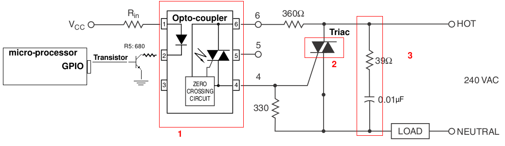
A light-dimming control system is being developed for a 240V heat lamp with a power dissipation of approximately 250W. The objective is to adjust the heat output of the lamp using control from a microprocessor. The development is based...