
et1602 circuit diagram

The laptop schematic circuit diagram serves as a crucial resource for technicians and engineers involved in laptop repair and maintenance. This diagram provides a detailed representation of the electrical connections and components within a laptop, allowing for systematic troubleshooting and repair processes.
The schematic typically includes various sections such as power management circuits, processor connections, memory interfaces, and peripheral component interconnects. Each component is represented with standardized symbols, and the connections between them are illustrated with lines that denote electrical pathways.
In the context of BIOS password removal, the schematic can be particularly beneficial. It may highlight specific points in the circuit where technicians can access the BIOS chip or related components to reset or bypass the password protection. This process often involves understanding the role of the EEPROM (Electrically Erasable Programmable Read-Only Memory) where the BIOS settings, including passwords, are stored.
Moreover, the schematic may include notes on voltage levels and signal paths, which are essential for diagnosing issues such as power failures, boot problems, or hardware malfunctions. Understanding these elements allows for effective repairs and modifications, ultimately enhancing the performance and longevity of the laptop.
Overall, a comprehensive laptop schematic circuit diagram is an invaluable tool that aids in the efficient repair and maintenance of laptops, facilitating a deeper understanding of their intricate electronic systems.Laptop Schematic Circuit Diagram for Laptop Repair, Laptop Bios Password Remove.. 🔗 External reference
Related Circuits
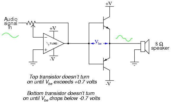
This project is an audio amplifier designed to amplify output signals from small radios, tape players, CD players, or other audio signal sources. For stereo operation, two identical amplifiers must be constructed—one for the left channel and another for...
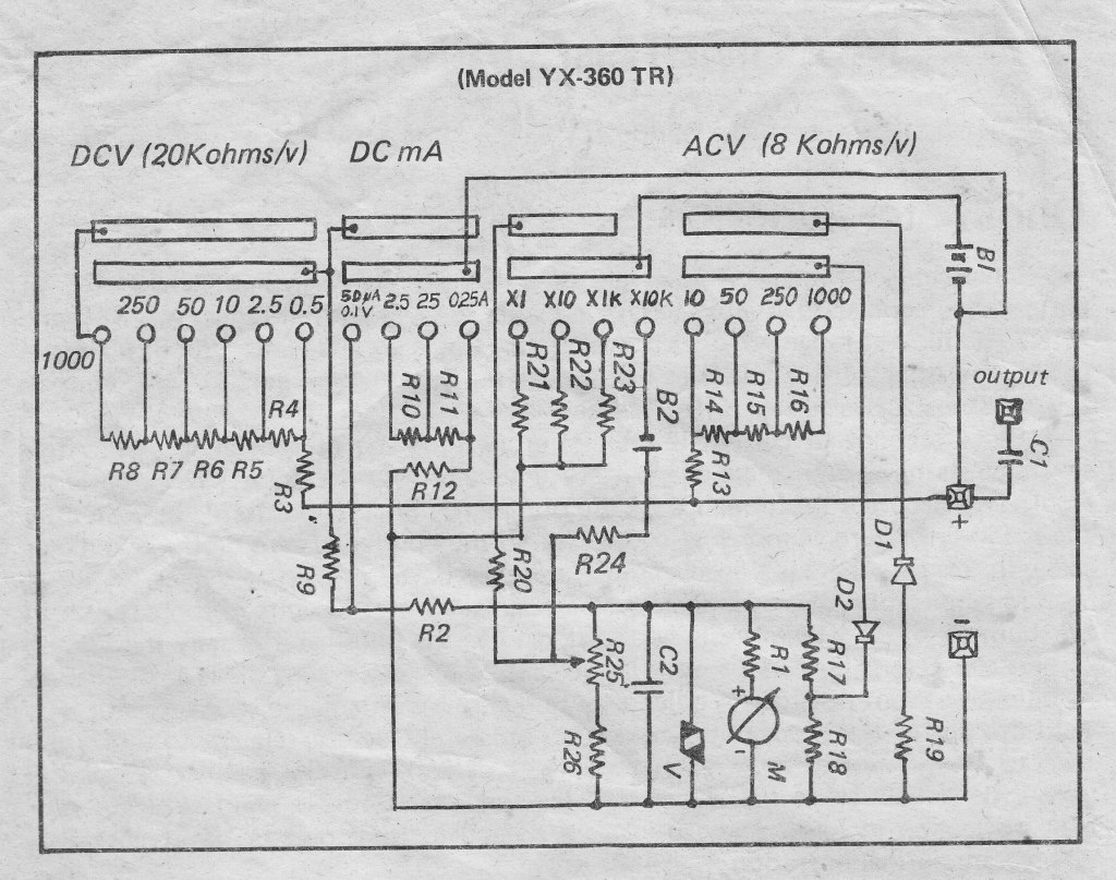
For individuals seeking a copy of the schematic diagram for this type of Analog Multitester, as well as other brands utilizing the same circuit diagram. The schematic diagram of an Analog Multitester typically features a variety of components arranged to...
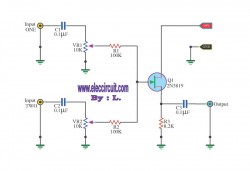
This circuit is a simple mixer circuit that can mix two signal channels into one output channel. It utilizes a codec circuit to convert stereo audio into mono audio. Additionally, the circuit can increase the number of channels by...
The circuit is activated by an LED/photoresistor isolator (U1), which combines a light-dependent resistor (LDR) and an LED in a single package. This device was selected for its high isolation characteristic of 2000 V, which is essential since the...
Integrated circuit gates IC1-a and IC1-b form a monostable multivibrator, whose time constant is determined by capacitor C2 and resistor R3. When the transmitter is dekeyed and then almost immediately rekeyed, point TX+ goes low, causing pin 1 to...
This is a cost-effective circuit that incorporates precise current limiting functionality into a voltage regulator. The circuit described is designed to enhance the performance of a voltage regulator by integrating a current limiting feature. This is particularly beneficial in applications...