
F007 excellent performance of low-frequency signal generator circuit

The low-frequency signal generating circuit is designed to operate efficiently across a wide frequency range, making it suitable for various measurement applications. The core of the circuit is the operational amplifier, which plays a crucial role in signal amplification and shaping. The feedback network, specifically configured as a Venturi oscillator, allows for precise control over the oscillation frequency, ensuring that the output signal remains stable and reliable.
The complementary push-pull amplifier configuration at the output stage is essential for driving heavier loads, enhancing the circuit's versatility in practical applications. The choice of components, such as resistors (R4), capacitors (C1), and the potentiometer (W1), is critical in determining the performance characteristics of the circuit. The negative feedback mechanism implemented with these components serves to stabilize the output amplitude and reduce distortion, which is vital for accurate signal generation.
Adjustments to the output amplitude can be easily made through the potentiometer, allowing users to tailor the signal output to specific requirements. The design also emphasizes the importance of maintaining the relationship between R1 and C1 to limit waveform distortion, ensuring that the generated signals are as clean and precise as possible.
Overall, this low-frequency signal generating circuit is a robust solution for applications requiring stable and high-quality low-frequency signals, with specifications that cater to a wide range of operational needs. Its design principles and component selection contribute to its effectiveness as a measurement signal source, making it an invaluable tool in electronic testing and analysis. As shown for the excellent performance of the low frequency signal generating circuit. The characteristics of this circuit is leveled good performance, high output power, wavef orm distortion, it is an ideal low-frequency measurement signal source. The figure, the operational amplifier A: Their feedback network of a typical venturi oscillator, the oscillation frequency is:f0 1/2 RC A2 output terminal OCL complementary push-pull amplifier is connected to increase the load capacity of the circuit. The operational amplifier A1 connected to the negative half-wave amplifier with W1, R4, C1, T1 and other elements constituting the negative feedback circuit leveled.
Either adjust the potentiometer output amplitude W1, and acts as a sampler in the feedback loop. In order to ensure a small waveform distortion, the general should make R1C1 20 RC.The circuit output amplitude is 0.5 ~ 5V, output current 0 ~ 1A, frequency adjustment range of 10Hz ~ 10kHz, output resistance is less than equal to 0.05, harmonic distortion is less than 0.1%.
Related Circuits

The filter consisting of resistors R1, R2, and capacitor C1 integrates the PWM waveform. The purpose of the operational amplifier appears to be that of a non-inverting amplifier, with the gain determined by resistors R6 and R7. However, the...
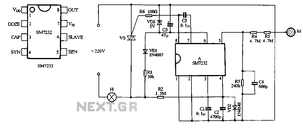
The core component of the circuit is the dimmer, utilizing the SM7232 integrated circuit. The pin configuration includes: 1) VDD, the positive power supply terminal; 2) DOZE; 3) CAP; 4) SYN, which synchronizes input power frequency using an internal...
How the processor produces 3 as the output. This question may be challenging to answer in simple terms. If so, a link to a book would be helpful. The process by which a processor generates the output of the number...
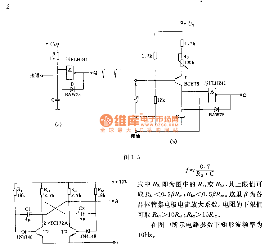
The circuit consists of two components whose parameters and models are designed to simultaneously generate a rectangular wave with a duty cycle of 1:1. The frequency is defined by the equation f = 0.7/(RB * C), where RB refers...
The switch circuit consists of a capacitive oscillator, an integration network, and a comparator circuit that controls a relay. When a body comes close to the induction plate, the inductive capacitance to ground increases, causing the 555 astable multivibrator...
The amplifier circuit utilizing the STK4050 integrated circuit (IC) is known for its robustness and high quality. This article presents a 200-watt power amplifier circuit based on the STK4050. The circuit features an advanced auto wiring diagram with color-coded...