
Fast Pulse Detector

The fast pulse detector circuit is designed to accurately identify and process rapid pulse signals, making it suitable for applications in digital communications, radar systems, and high-speed data acquisition systems. The key components of the schematic typically include a high-speed comparator, a pulse shaping circuit, and a signal conditioning stage.
The high-speed comparator is essential for detecting the presence of the pulse. It compares the incoming signal against a predefined threshold level. When the signal exceeds this threshold, the comparator outputs a logic high signal, indicating the detection of a pulse. The choice of comparator is critical, as it must have a fast response time to handle the 60 ns pulse width effectively.
Following the comparator, the pulse shaping circuit refines the detected signal to ensure that it has a clean rise and fall time, which is crucial for subsequent processing stages. This may involve the use of resistors and capacitors to form an RC network that filters out noise and reduces ringing.
The signal conditioning stage may include additional filtering, amplification, and level shifting to prepare the signal for further processing or interfacing with digital logic circuits. This stage ensures that the output signal maintains integrity and is compatible with the input requirements of downstream components.
Overall, the design of the fast pulse detector circuit emphasizes speed and accuracy, achieving an error detection rate of less than 10% for 60 ns pulses, thus facilitating reliable operation in high-speed applications. Proper layout and component selection are vital to minimize propagation delays and ensure the circuit's performance meets the specified criteria.A schematic diagram of a fast pulse detector is show in the figure below. Error detection rate under 10% can be expected for 60 ns pulse. To get error free.. 🔗 External reference
Related Circuits
The GLMDPCB motion detector board is a double-sided etched, screened, and drilled printed circuit board designed for the GLMDA motion detector circuit illustrated in the schematic below. The circuit can be constructed in its entirety or in part. For...

Clipping is a significant issue that leads to distortion in amplifiers. It results in the amplitude level of a waveform dropping abruptly before it reaches its intended limit. This document presents a straightforward circuit designed to detect clipping in...
This circuit responds to RF signals below the standard broadcast band up to over 500 MHz and provides both visual and audible indications when an RF signal is detected. By adjusting the bias of diode D2 with the R2...
The HCS12 series of microcontrollers does not include dedicated internal digital-to-analog conversion hardware. Therefore, external hardware, such as a digital-to-analog conversion integrated circuit (IC), is required. To implement digital-to-analog conversion (DAC) in systems utilizing the HCS12 microcontroller, an external DAC...
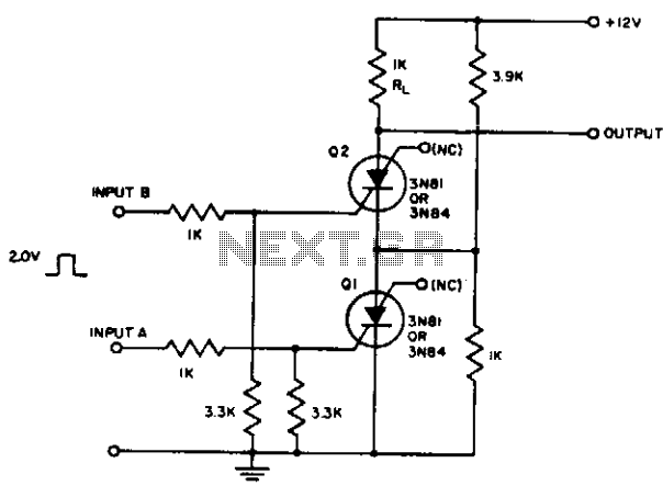
The resistor divider connected between Q1 and Q2 supplies IH to Q1 after input A triggers it. It also prevents the input from triggering Q2 until Q1 conducts. Consequently, the first input pulse after input A is applied will...
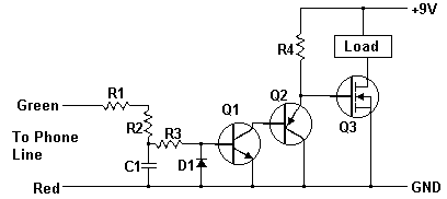
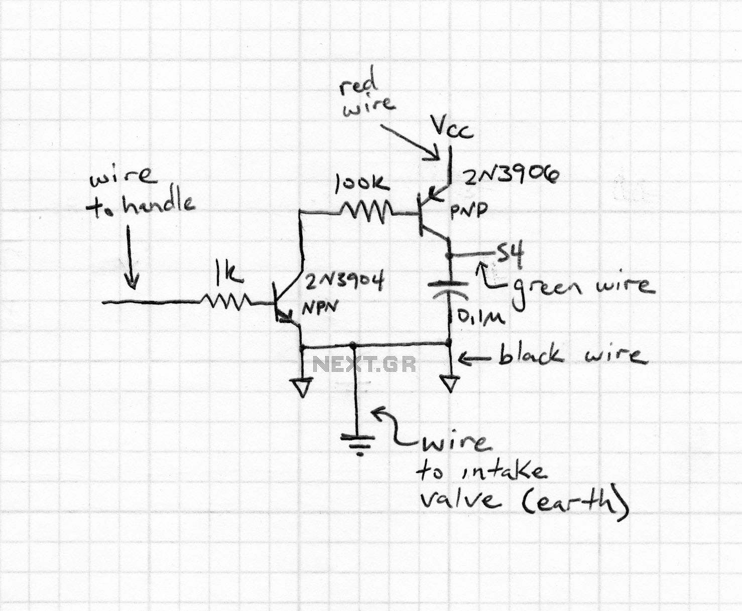
A while ago I got an email asking for the schematic of a circuit to detect cut phone lines. It didn’t take me long to find this circuit in Electronics Now. When the circuit detects that a phone line...