
Five-transistor amplifier

The circuit is designed to operate efficiently across a frequency range from DC to 50 MHz, making it suitable for high-speed applications. The use of a TTL signal to drive the circuit ensures compatibility with digital logic levels, allowing for straightforward integration into existing systems. The 740S00 quad Schottky NAND gate provides fast switching characteristics due to its Schottky diode technology, which minimizes propagation delay.
Transistor Q1, as a common-emitter amplifier, amplifies the input signal, providing a necessary gain before driving the subsequent stages. The configuration of Q2 as an emitter follower allows for impedance matching, ensuring that the signal is transferred effectively to the output stage without significant loss.
The parallel configuration of transistors Q3 and Q4 enhances the output drive capability, allowing for a stronger output signal while maintaining low output impedance. The role of transistor Q5 as a low-impedance sink is critical in maintaining signal integrity, especially during transitions when Q3 and Q4 are turned off.
The inclusion of Schottky diodes D1 and D2 is essential for protecting the circuit from saturation, which could lead to distortion or unwanted signal behavior. The adjustment of potentiometer R1 allows for fine-tuning of the output pulse characteristics, particularly its fall time, which is crucial for high-speed signal applications.
Inductor L1 serves as a peaking coil, and its adjustment is vital for optimizing the rise time of the output pulse. This ensures that the signal remains within the desired overshoot limits, which is important for preventing signal integrity issues in high-frequency applications. The ability to vary capacitor C1 provides additional control over pre-shooting, allowing for further refinement of the output signal.
Capacitor C2 plays a significant role in shaping the output pulse, allowing for additional fine-tuning of the signal waveform. The resistors R2 and R3 are strategically placed to ensure a consistent 50-ohm impedance at the amplifier's output, which is crucial for minimizing reflections and maximizing power transfer in RF applications. This impedance matching is particularly important in high-frequency circuits to maintain signal fidelity and prevent degradation of the output pulse quality.The circuit works from dc to 50 MHz and will deliver pulses as short as 10 ns. It is driven by a TTL signal through a 740S00 quad Schottky NAND gate, ICA through ICD. Transistor Ql, wired as a common-emitter amplifier, drives transistor Q2, a simple emitter follower. Transistors Q3 and Q4, wired in parallel, also form an emitter follower and drive the output. When Q3 and Q4 are both turned off, transistor Q5 works as a low-impedance sink. Schottky diodes Dl and D2 prevent Ql and Q5 from becoming saturated. To adjust the circuit, potentiometer Rl is set to optimize the output pulse's fall time. Inductor LI, a peaking coil, should be adjusted to improve the rise time to within a permissible 5% overshoot. Likewise, capacitor CI can be varied to control pre-shooting. Further output pulse shaping is accomplished with the help of capacitor C2. Resistors R2 and R3 ensure a proper 50-ohm impedance at the amplifier's output when the pulse is on or off, respectively.
Related Circuits
The circuit presented is experimental and should provide some fun to build and play about with. It has been built and tested and works very well indeed. Please note that it is a low current Class-A opamp and is...
This design is based on an 18 Watt Audio Amplifier and was developed primarily to address the needs of users who have difficulty locating the TLE2141C chip. It utilizes the commonly available NE5532 Dual IC; however, its power output...
The basis for this amplifier has been around now for several years as Project 3A, and requires only relatively small modifications to be able to operate in Class-A. The biggest change is in output power (reduced dramatically from the 60-100W...

This circuit is capable of delivering approximately 200W of power output, produced by Phillips Semiconductor. It utilizes two PHP1BN11QT devices and operates with an input voltage range of 30 to 45 Volts DC. The described circuit is a high-power switching...
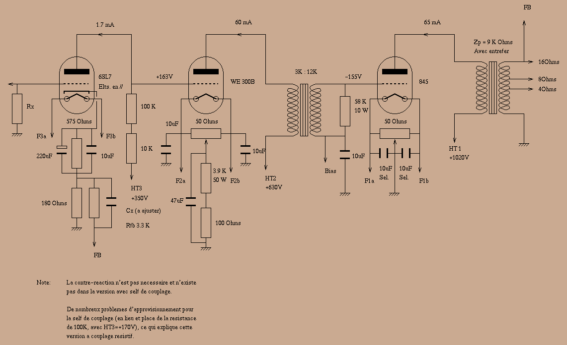
This project is finalized, that means it is no longer experimental. This amplifier, although limited in output power (20W), has been designed to give the best listening pleasure. No compromise has been made during components choice: the 845 output...

Integrated circuits (ICs) are commonly utilized in various audio amplifiers, particularly in compact circuits. While transistors are convenient alternatives, they offer several advantages, such as the ability to repurpose old equipment to create smaller circuits, which may be harder...