
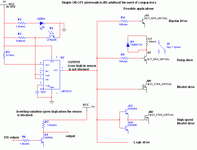
Flip-Flop Debouncer Switch

This circuit design employs a dual D-type flip-flop, specifically the 74HC74, which is integral for creating a simple binary counter. The configuration is designed to provide reliable operation while minimizing the effects of switch bounce. The use of IC1A as a true/complement buffer allows for clear differentiation between the binary states.
Resistors R1 and R2 play critical roles in the reset timing of the flip-flop. They ensure that the output of IC1A is stable and ready for clock input by delaying the reset state just enough to synchronize with the clock edge. This timing is crucial in digital circuits where precise control over state changes is necessary.
The logic state of IC1A is routed to pins 1 and 3 through R3, which acts as a pull-up or pull-down resistor, depending on the design requirements. This arrangement guarantees that the correct logic level is applied to the flip-flop inputs, thus ensuring accurate counting.
When the switch is pressed, it triggers a transition that allows the stored charge in the capacitor to dictate the reset and clock inputs of the flip-flop. This mechanism effectively captures the intended state change without delay. Upon releasing the switch, the capacitor, in conjunction with resistor R4, charges to the next state, preparing the circuit for the subsequent logic operation.
The outputs of IC1A and IC1B provide the binary representation of the counter's state, with IC1A yielding the least significant bit and IC1B yielding the most significant bit. This design choice facilitates easy integration into larger digital systems where multi-bit binary values are necessary.
The unique characteristic of this circuit is its ability to increment the counter state on the initial press of the switch rather than on its release. This feature distinguishes it from traditional switch-debouncing techniques, which often rely on the release action to register a state change, thus enhancing responsiveness in applications where timing is critical.
The option to replace R1 with a 22-pF capacitor offers an additional layer of flexibility. By doing so, the circuit's sensitivity to parasitic capacitance is reduced, which can be particularly beneficial in high-frequency applications. Furthermore, this modification allows for a proportional reduction in the resistance values of R2 and R3, leading to a more compact and efficient design.
Overall, this circuit exemplifies a robust approach to implementing a binary counter using flip-flops, with considerations for noise immunity and timing precision. Although this circuit uses a 74HC74, any CMOS variant of this flip-flop will work. IC1A acts as a true/ compleme nt buffer. RI and R2 ensure that IC1A comes out of reset before the clock"s edge occurs. R3 applies IClA"s logic state to pins 1 and 3. When the switch closes, the next logic state stored on the capacitor transfers to the flip-flop"s reset and clock inputs. Releasing the switch lets the capacitor charge to the next state via R4. IClA"s output is the LSB; IClB"s output is the MSB. Notice that the counter"s state advances when the switch is first pressed, rather than when it"s released; the latter is the case with many other switch-debouncing schemes.
You can replace RI with a 22-pF capacitor to reduce the circuit"s sensitivity to parasitic effects. The addition of this capacitor also lets you lower the magnitude of R2 and R3 by a factor of 10.
Related Circuits
The 555 timer is recognized as one of the most versatile and widely used integrated circuits globally. One of its potential applications is as a simple inverting Schmitt trigger. The 555 timer can be configured in various modes, including monostable,...
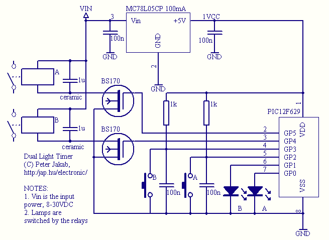
This is a lamp timer capable of operating two separate relay switches. Outputs can be in three (or restricted to two) states: OFF, delayed ON and constant ON. Delayed ON mode is indicated by the LEDs. The source code...

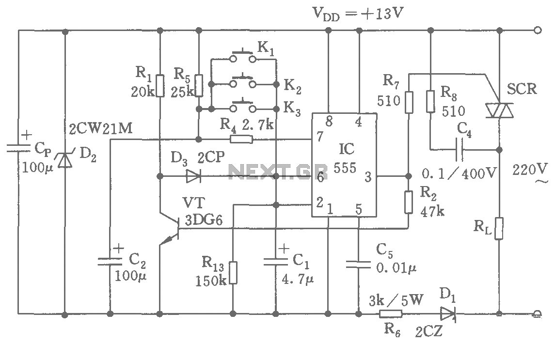
This modulated triac zero-point switching circuit controls heater loads operating from 115 Vac. Circuit operation is best described by splitting the circuit into two parts. The circuit on the right is the zero-point switch; to the left is the...

The circuit below uses a CMOS dual D flip flop (CD4013) to toggle a relay or other load with a momentary push button. Several push buttons can be wired in parallel to control the relay from multiple locations. A...

This Project REMOTE CONTROLLED SWITCH BOARD is used to switch on/off the Home Appliances by using a standard Remote control. The system is used to switch on/off up to six electrical devices. All the above processes are controlled by...
The switching circuit consists of a buck rectifier circuit, a bistable trigger circuit, and a thyristor control circuit, enabling remote control for electrical equipment to be turned on or off. The buck rectifier circuit supplies the controller with a...