
flyback with a pulsed DC signal

The circuit utilizes a 555 timer IC configured in astable mode to generate a square wave signal at a frequency of approximately 15.76 kHz, which is suitable for applications such as driving a flyback transformer. The power supply connections for the 555 timer are critical; pin 1 is connected to ground, while pin 8 is connected to a +12V supply. These connections are essential for the proper operation of the timer.
The output from the 555 timer is fed into a PNP transistor, designated as Q1, which acts as a switching device to control the larger power transistor, Q2, a 2N3055 NPN transistor. This configuration allows the circuit to handle significant current loads, as the 2N3055 can switch over an amp during operation. It is important to note that Q2 must be equipped with an adequate heatsink to dissipate the heat generated during operation, preventing thermal overload and ensuring reliable performance.
The output terminals from the 2N3055 transistor are connected to the primary winding of a flyback transformer. Flyback transformers are known for their ability to generate high-voltage outputs, and they typically feature multiple primary terminals—up to ten—and a single secondary terminal. The secondary terminal is easily identifiable as the thick, insulated wire protruding from the top of the unit, which is designed to handle high-voltage outputs.
Selecting the appropriate primary terminals for the flyback transformer often requires experimentation. The effectiveness of the connection can be assessed by observing the size of the arc produced at the secondary terminal. A bench power supply providing 12V is recommended for powering the circuit, allowing for controlled adjustments to the oscillator frequency to achieve optimal performance.A 555 is used as an oscillator, optimally around 15.76KHz (in North America). Power pins on the chip (pin 1 to ground, pin 8 to +12V) are not shown on the diagram. The output from the 555 is then switched by PNP transistor Q1 and by the large 2N3055 NPN power transistor. Q2 must be adequately heatsinked as well since it may well switch over an amp during operation. Output terminals are then connected to a primary winding of the flyback. The average flyback has up to ten primary terminals and one secondary (the secondary identified as the thick, insulated, wire protruding from the top of the unit).
Choosing the correct primary terminals is usually a matter of trial-and-error with the effect evaluated by the size of the arc produced! Connect a 12V supply to the circuit (a bench-type supply works well here), set the oscillator frequency to something i
🔗 External reference
Related Circuits

This device is a high-quality RF signal meter utilizing the Analog Devices AD8313 logarithmic detector integrated circuit (IC), which operates within the frequency range of 0.1 GHz to 2.5 GHz. It can detect signals as low as -80 dBm....

The ADC0804 converts the output voltages from the LM34/LM35 temperature sensors into digital signals that correspond to the measured temperature. These digital signals are then processed by the 8051 microcontroller. The temperature range for the LM35 sensor is from...
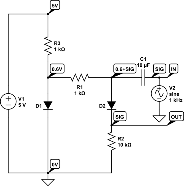
D1 compensates for the forward voltage drop of D2 by providing a 0.6V bias. The +5V is an external source. D1, R1, and R3 create a 0.6V bias on the capacitor's other side, allowing a positive signal swing to...

This is a simple circuit that can be used as a sequential signal light in automobiles. The circuit is based on two integrated circuits (ICs): a TS 555 CN CMOS timer IC and a CD4017 decade counter IC. The...
This signal generator is designed for the realignment of radio receivers. The unit is inexpensive and relatively simple but adequately serves its intended purpose. However, the output is not a pure sine wave, which may make it unsuitable for...

A 1488 kHz master oscillator quartz crystal resonator is utilized for frequency stabilization. The output from the frequency divider provides three different square wave signal outputs at 4 kHz, 12 kHz, and 124 kHz. The circuit includes transistors VT1,...