
fm antenna booster circuit

The FM antenna booster circuit is designed to enhance the reception of FM radio signals, particularly from distant stations, by amplifying weak signals for clearer audio output. The core component of this circuit is the 2SC2570 transistor, which operates as a common-emitter RF preamplifier. This configuration is known for its ability to provide significant voltage gain while maintaining a relatively low noise figure, making it suitable for radio frequency applications.
The circuit layout should be implemented on a high-quality printed circuit board (PCB), preferably made of glass-epoxy material, which offers good thermal and electrical properties. The use of a well-constructed PCB minimizes parasitic capacitance and inductance, which can adversely affect performance at VHF/UHF frequencies.
Adjustable trimmers VC1 and VC2 are integral to the circuit, allowing for fine-tuning of the input and output stages, respectively. Proper adjustment of these components is crucial for achieving maximum gain and optimal performance.
The input coil L1, made with four turns of 20 SWG enamelled copper wire, is wound slightly spaced over a 5mm diameter former. This specific construction helps in tuning the circuit to the desired frequency range. The tapping point at the first turn from the ground lead side allows for flexible adjustment of the input signal level, further enhancing the circuit's adaptability.
Coil L2, which consists of three turns of similar wire, serves a complementary role in the circuit, contributing to the overall impedance matching and frequency response. The careful design of these coils is essential for maximizing the efficiency of the antenna booster.
The pin configuration of the 2SC2570 transistor should be referenced from the schematic to ensure correct connections and optimal operation of the circuit. Overall, this FM antenna booster circuit provides an effective solution for improving FM reception, making it a valuable addition for users seeking to enhance their radio listening experience.This is a design circuit for a low cost fm antenna booster that can be used to listen to programs from distant FM stations clearly. The antenna fm booster circuit comprises a common-emitter tuned RF preamplifier wired around VHF/UHF transistor 2SC2570 (C2570).
This is the figure of the circuit; Assemble the circuit on a good-quality PCB (preferabl y, glass-epoxy). Adjust input/output trimmers (VC1/VC2) for maximum gain. Input coil L1 consists of four turns of 20SWG enamelled copper wire (slightly space wound) over 5mm diameter former. It is tapped at the first turn from ground lead side. Coil L2 is similar to L1, but has only three turns. Pin configuration of transistor 2SC2570 is shown in the fm antenna booster schematic. 🔗 External reference
Related Circuits
Samsung C3330 Circuit Diagram Download Manual PDF Download. The Samsung C3330 circuit diagram serves as a comprehensive reference for understanding the electronic architecture of the device. This schematic provides detailed insights into the interconnections between various components, including the microcontroller,...

Measurements were conducted using a modified program to measure the voltage applied at the drive electrode and the voltage at the sense electrode. Conductance was calculated using the formula 0.01S * V_resist / (V_applied * V_resist). The initial version...
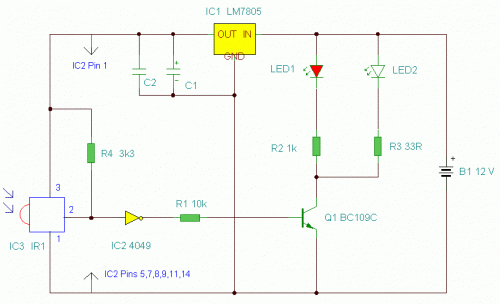
This is an enhanced infrared (IR) remote control extender circuit. It features high noise immunity, resistance to ambient and reflected light, and an extended range of approximately 7 meters from the remote control to the extender circuit. It is...
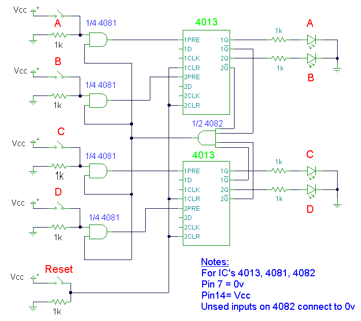
This design utilizes four integrated circuits (ICs) and features four input circuits with four independent outputs, along with a single master reset switch. The outputs are configured with light-emitting diodes (LEDs), which can be modified to control lamps or...
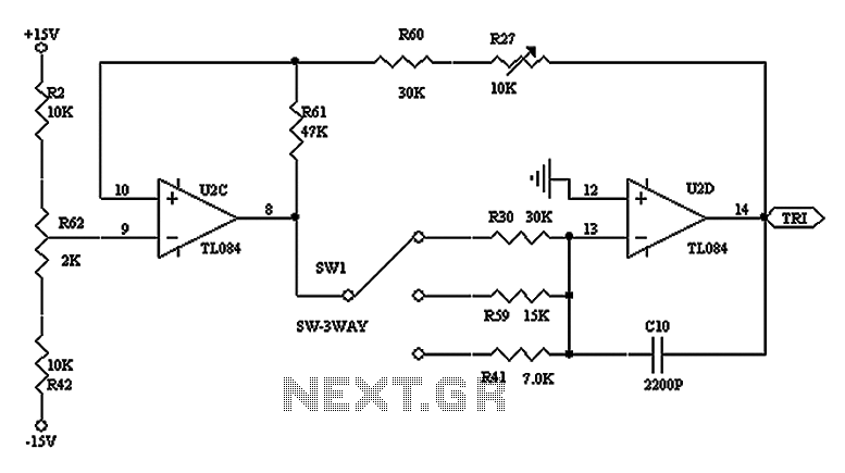
The triangular wave circuit consists of two operational amplifiers (OPs). R62 serves as the offset adjustment, while R27 is utilized for peak adjustment. A switch is included to select different resistances, allowing for the generation of triangular waves at...
A dimmer is a simple device used to reduce the brightness of incandescent lamps and to control the speed of collector motors. This concept has gained popularity due to the abundance of outdated Soviet circuits available on Lithuanian internet...