
Quiz Circuit

The schematic design includes a power supply section capable of accommodating a voltage range from 3 to 15 volts, ensuring versatility in the choice of components. The use of CMOS technology allows for low power consumption and high noise immunity, making it suitable for battery-operated devices. The core of the design is the dual 4013 D-type flip-flop, which serves as a bistable latch. This flip-flop is crucial for maintaining the state of the output LEDs based on user interaction with the input switches.
The four input switches are connected to the two-input AND gates (4081) that receive signals from the four-input AND gate (4082). The logic flow ensures that only one LED can be activated at a time, providing a clear visual indication of which switch has been pressed. The reset function is integrated into the circuit through a dedicated switch that, when activated, resets all flip-flops and extinguishes the LEDs, returning the circuit to its idle state.
The design also incorporates a simple yet effective mechanism to prevent multiple inputs from being registered simultaneously, enhancing the reliability of the circuit. The heavy-duty push-button switches recommended for this design are essential for ensuring long-term durability and performance, especially in applications where the switches may undergo frequent use. Overall, this circuit provides a straightforward and efficient solution for applications requiring single-output control from multiple inputs, with the flexibility to adapt the output devices as needed.This design uses four IC`s and has four input circuits and four independent outputs and a single master reset switch. The outputs here are LED`s but may be modified to drive lamps or buzzers. Only one output LED can be lit at any time. The first person to press their input switch, A, B, C, D will light the corresponding output LED, disabling the other inputs.
The circuit uses all CMOS IC`s part numbers shown on the diagram. The supply voltage may be anything between 3 and 15 volts. Alternatively, it may be built using equivalent TTL IC`s and powered on 5 volts. The main component in this circuit is a bistable latch, here it is based on the dual 4013 D-type flip flop. Pressing the reset switch will clear all flip flops and extinguish any lit LED`s. Under this condition the Q outputs will all be low (logic 0) and NOT Q outputs will be high (logic 1).
All four NOT Q outputs are fed to a 4 input AND gate, the 4082 whose output will also be high. The output of the 4082 is wired to one input of each 2 input AND gate (4081). Switch inputs A, B, C, D are all non latching push button switches, the first person to press their switch will cause the corresponding AND gate (4081) to go high and trigger the preset input of the 4013 D-type flip flop. This will latch and light the appropriate LED. Also the triggered flip flop will have its NOT Q output, set at low, this changes the 4082 output to low and prevents any further triggering of the other flip flops.
Switch contact de-bouncing is not required as the first press will latch one of the bistables. Pressing the reset switch, restores the circuit to its former state. I would recommend using heavy duty push button switches, as in use they are likely to be under some stress. 🔗 External reference
Related Circuits
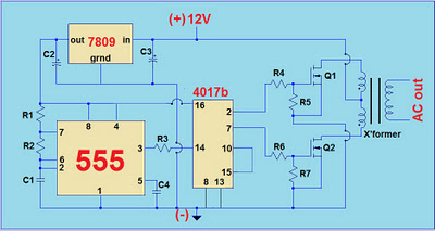
This project involves a simple 12V to 220V modified sine-wave inverter utilizing a 555 timer IC and a CD4017 decade counter. The inverter is capable of delivering 300W of continuous power and approximately 500W of maximum power output for...
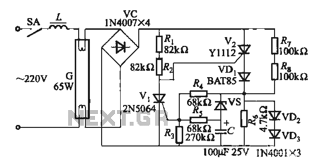
One electronic ballast circuit is depicted in Figure 2-11. This circuit utilizes a specialized fluorescent lamp starter thyristor, SCR Y1112, which is superior to ordinary thyristors due to its ability to maintain a higher current value and dU/dt values....
Section Ul-a is configured as a high-gain inverting voltage amplifier that is inductively coupled to the phone line via LI. Inductor LI is a homemade unit that consists of 250 turns of fine, enamel-coated wire that is wound on...

This circuit generates a digital square wave that can be displayed directly or utilized to drive additional circuits. It employs the CMOS 4047 Low-Power Monostable/Astable Multivibrator, as referenced in Tom Duncan's "Adventures with Digital Electronics" book, to control a...
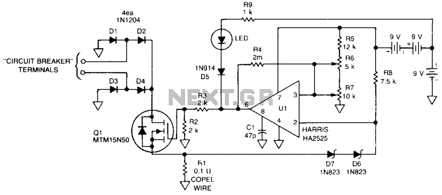
This 115 Vac electronic circuit breaker utilizes the low drive power, low on-resistance, and fast turn-off characteristics of the TMOS MTM15N50. The trip point is adjustable, and an LED fault indication is provided, with battery power ensuring complete circuit...
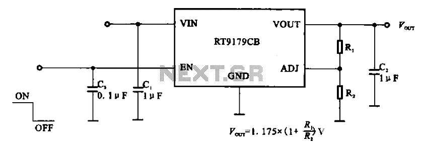
The RT9179CB is a power management chip utilized in power supply circuits. It serves as a linear regulator power management chip. This circuit is commonly employed in various products, such as computer motherboards, LCD monitors, and others. It is...