
fm antenna booster circuit diagram

The input coil L1 plays a crucial role in the circuit as it serves to couple the RF signal into the transistor amplifier stage. The use of 20 SWG enamelled copper wire ensures that the coil has a suitable inductance and resistance for effective signal transmission. The slightly spaced winding technique minimizes the capacitance between turns, thereby enhancing the coil's performance at radio frequencies.
Coil L2, with its three turns, functions similarly to L1 but is designed to provide a different inductance value, which can be beneficial for tuning the circuit to specific frequencies or for impedance matching purposes. The reduced number of turns in L2 results in lower inductance, which can be advantageous in certain applications where higher frequency response is required.
The transistor 2SC2570, utilized in this circuit, is a common NPN transistor known for its high frequency and low noise characteristics, making it suitable for RF applications such as FM antenna boosters. The pin configuration of the 2SC2570 is essential for proper integration into the circuit, ensuring that the collector, base, and emitter are correctly connected to optimize the transistor's performance.
Overall, the combination of the two coils and the transistor creates a tuned circuit that can amplify weak RF signals captured by the antenna, significantly improving reception quality. Proper attention to the winding technique, number of turns, and transistor configuration is critical in achieving optimal performance in FM antenna booster applications.Input coil L1 consists of four turns of 20SWG enamelled copper wire (slightly space wound) over 5mm diameter former. It is tapped at the first turn from ground lead side. Coil L2 is similar to L1, but has only three turns. Pin configuration of transistor 2SC2570 is shown in the fm antenna booster schematic. 🔗 External reference
Related Circuits
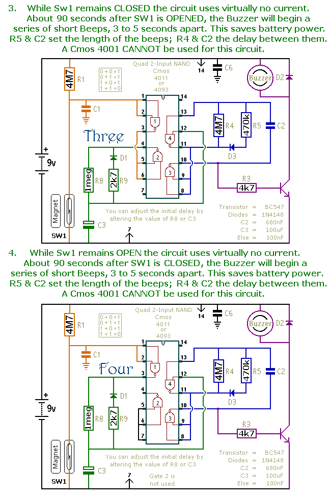
This document presents a collection of compact, self-contained alarm circuits. These circuits are designed to operate with a very low standby current, making them ideal for battery-powered applications. They can be triggered by both normally-open and normally-closed switches, while...
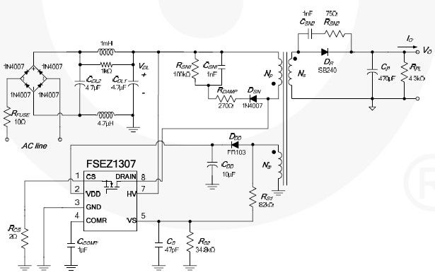
This cell phone charger circuit diagram electronic project is based on the FSEZ1307 third-generation primary side regulation (PSR) PWM controller integrated circuit. The FSEZ1307 cell phone charger can be used for battery charger applications for devices such as cellular...
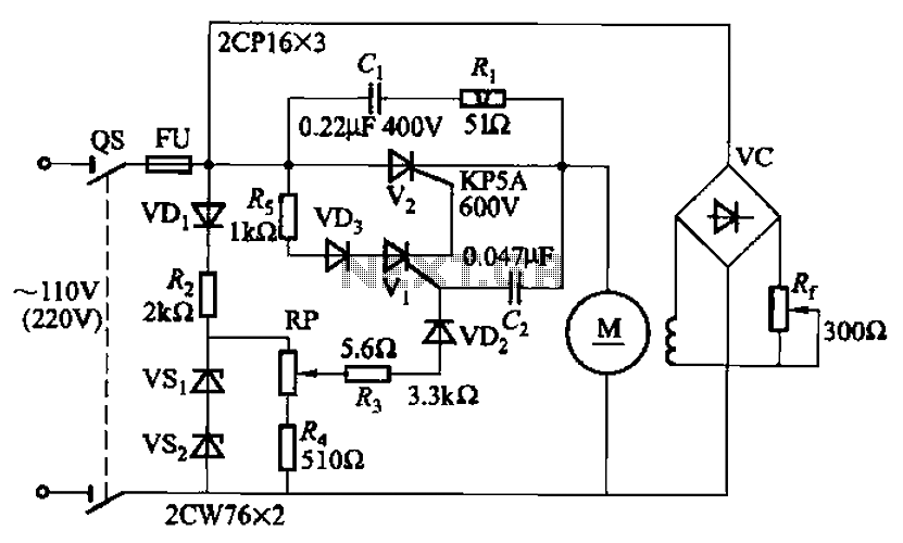
A 100W resistance-triggered motor control circuit designed for arc welding machines. It features an adjustment potentiometer (Rr) that can modify the DC motor excitation current. Additionally, a regulator (RP) is included to adjust the DC motor armature voltage, enabling...
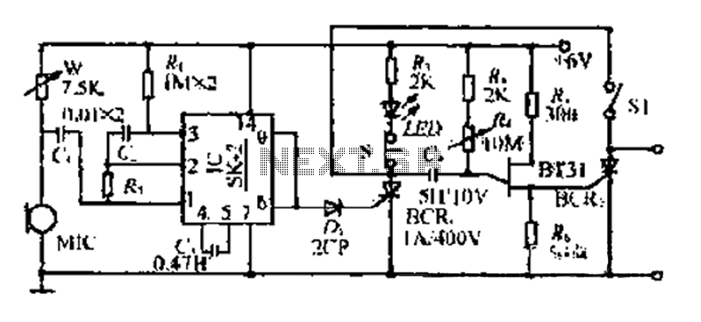
The circuit includes a microphone (MIC) housed in a cylindrical body that captures sound when an object makes contact. The audio signal is coupled to an integrated circuit (IC) for amplification. The output from the IC, at pins 6...
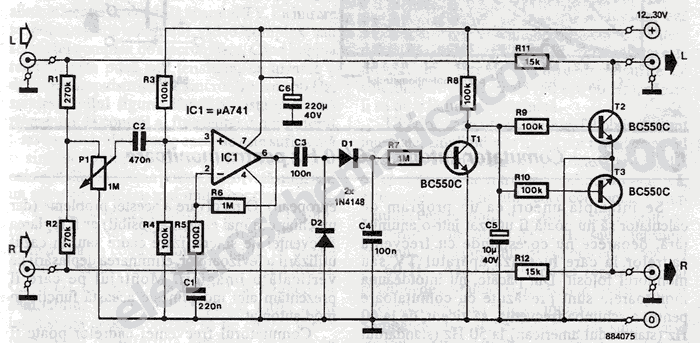
This stereo noise blanker or suppressor attenuates noise by 45 dB when the music signal is low or absent; it functions primarily as a noise limiter. The noise blanker sensitivity... This circuit serves as a stereo noise blanker or suppressor,...
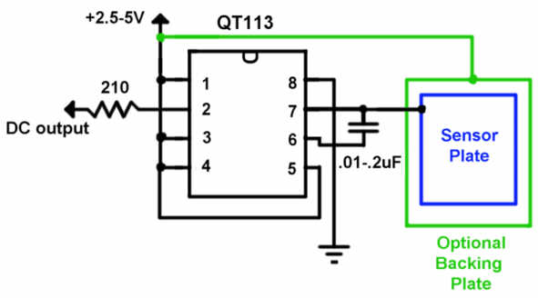
The QT113 is a capacitance touch sensor that does not require AC line voltage to operate. Instead, it detects changes in capacitance caused by the proximity of a user’s body. A sensor plate measuring 2 inches square can sense...