
FM modulator strong - weak signal switching circuit

The FM modulator circuit operates by utilizing a switching mechanism that adapts to varying signal strengths. The mechanical switches shown in diagram 3-14 (a) allow for user interaction, enabling the selection of the desired signal strength. This feature is particularly useful in environments where signal quality fluctuates, as it provides the operator with the flexibility to optimize reception.
The diode switching control illustrated in Figure 3-14 (b) plays a crucial role in managing the circuit's response to incoming signals. The diode's ability to switch between conducting and non-conducting states allows for efficient signal processing. When the signal strength is sufficient, the diode is forward biased, allowing the antenna to connect directly to the resonant circuit. This direct connection facilitates a stronger and clearer signal reception.
Conversely, when the signal is weak, the diode enters a reverse bias state, which activates a signal induction process via an inductor into the resonant circuit. This method results in a controlled attenuation of the signal, quantified at approximately 12 to 15 dB. Such attenuation is essential for preventing overload from strong local signals, ensuring that the circuit can effectively discriminate between strong and weak signals.
The intermediate frequency amplifying circuit, as shown in Figure 3-14 (c), is integral to the overall performance of the FM modulator. By amplifying the signal before it is processed through the switching mechanism, the circuit can maintain high fidelity in signal transmission and reception. This design is particularly advantageous in applications where both strong local broadcasts and weaker distant signals must be managed simultaneously, providing a robust solution for diverse signal conditions in FM modulation scenarios.It shows an FM modulator of a strong, weak signal switching circuit. The circuit ring 3-14 (a) shown in mechanical switches, one for the workers selector switch to choose based on the signal strength. Figure 3-14 (b) shows the use of diode switching control. Figure 3-14 (c) shows the use of an intermediate frequency amplifying circuit receives the signal level strength diode control. VT3 control diode bias, when forward biased channel antenna number directly into the resonant circuit, reverse bias to induction via the inductor to the resonant circuit, about 12 ~ 15 dB attenuation of the difference between the two.
This is generally used to attenuate the switching circuit receiving a strong signal (local broadcast) and weak signal (the signal field) antenna input.
Related Circuits
This circuit was designed approximately four months ago and has been developed into a kit for others to use. The circuit in question appears to be a well-thought-out design that has been packaged into a kit format, making it accessible...

A sensitive and reliable RF field strength meter is an invaluable instrument in amateur radio and radio-controlled model applications. This field strength meter is utilized to align antennas for optimal gain and to determine the transmission range of radio...
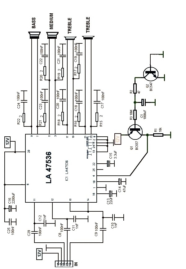
This car audio amplifier circuit is based on the LA47536 audio amplifier integrated circuit designed by Sanyo. This audio amplifier circuit is specifically designed for car audio power amplifiers. The LA47536 car audio amplifier IC features four output channels...

This circuit converts a sine wave into a square wave. It consists of a single 2-input NAND Schmitt trigger configured as an inverter, with an adjustable trigger level at its input. As the input voltage exceeds the gate's trigger...

Analyzing the three-phase winding involves examining the head and tail of various therapies, such as the use of hair bundles. The process is simple, safe, and quick. The analysis includes crimping electrical connections, as shown in FIG. 1. The...
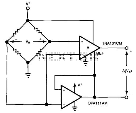
For systems with a single power supply, two operational amplifiers function as instrumentation and buffer amplifiers. The OPA111 AM buffers the reference mode of the bridge and applies that voltage to the reference terminal of the instrumentation amplifiers. The...