
Bridge Circuit With One Power Supply

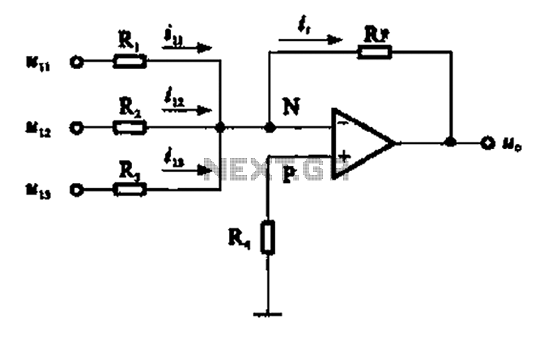
In this circuit configuration, the use of two operational amplifiers is critical for accurate signal processing. The first operational amplifier, configured as an instrumentation amplifier, amplifies the differential voltage from the bridge sensor while rejecting common-mode signals. This is essential in applications where the signal of interest is small compared to the noise levels.
The OPA111, known for its low offset voltage and low bias current, is particularly suitable for this application. It buffers the reference voltage from the bridge, ensuring stable and precise reference levels for the instrumentation amplifier. By applying this buffered reference voltage to the reference terminal of the instrumentation amplifier, the circuit minimizes any potential errors that could arise from fluctuations in the reference signal.
The output configuration, which takes the difference between the outputs of the two amplifiers, effectively cancels out the fixed output offset. This is a crucial design feature, as offset errors can significantly impact the accuracy of measurements in sensitive applications.
The additional operational amplifier serves to introduce a controlled bridge error. This is achieved by adjusting the gain of the amplifier to account for the bias current (IB) flowing through the bridge circuit. The relationship IB = V/R, where V is the voltage across the bridge and R is the resistance of one leg of the bridge, highlights the importance of precise resistance values in the bridge configuration. By carefully selecting the resistances and bias currents, the circuit can be calibrated to achieve optimal performance.
Overall, this circuit design is well-suited for applications requiring precise measurement and amplification of low-level signals, such as in sensor systems and data acquisition modules. The combination of instrumentation and buffer amplifiers, along with careful attention to bias currents and output configurations, ensures high fidelity in signal processing. For systems with only one power supply, two op amps act as instrumentation and buffer amps. The OPA111 AM buffers the reference mode of the bridge and applies that voltage to the instrumentation amps ref terminal. Output is taken between the amplifier outputs to exclude the fixed output offset. The additional op amp creates a bridge error of 2, where IB=bias current of op amp and R is the resistance of one leg of the bridge.
Related Circuits
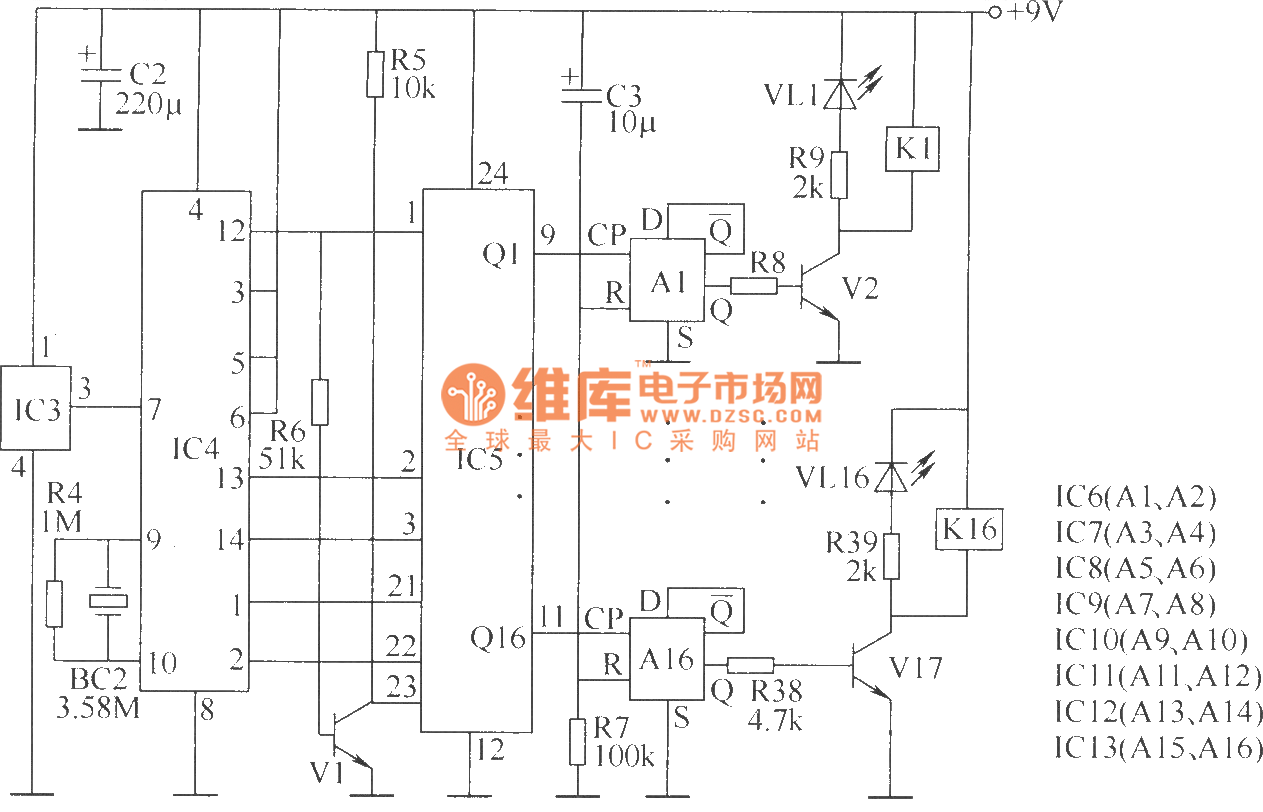
The wireless remote control transmitter circuit consists of control buttons S1 to S16, resistors R1 to R3, a capacitor C1, a regulator diode VS, a crystal oscillator BC1, and DTMF encoder integrated circuits IC1 and IC2. The circuit components...

Introduction The SP6648 integrated synchronous boost regulator is a compact circuit that provides ultra-high efficiency drive current for an LED flashlight using a Luxeon I light source. The circuit is configured to deliver a constant output current of 350mA...
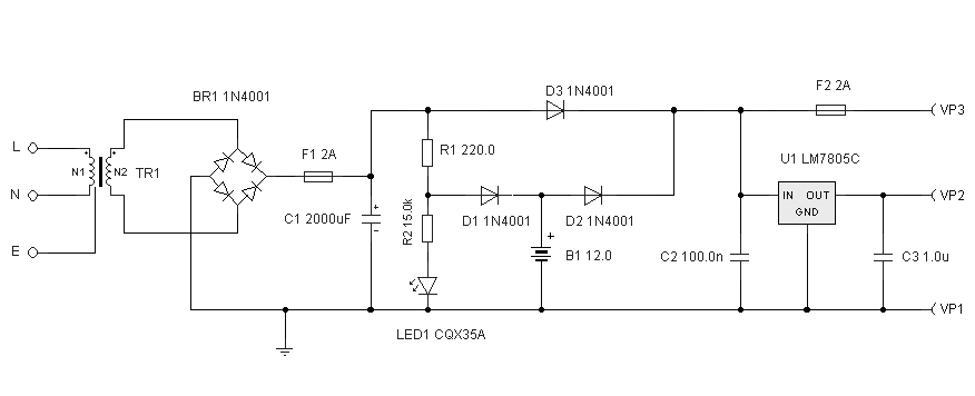
The circuit illustrated relates to a standard industrial UPS (Uninterruptible Power Supply), demonstrating how the batteries assume control during an electrical outage. The Uninterruptible Power Supply (UPS) circuit typically consists of several key components that ensure a reliable power supply...
An adder circuit, specifically the inverting adder circuit, utilizes the inverting input of an operational amplifier to process signals. Voltage inputs are added through resistors connected to the inverting input terminal of the operational amplifier. The circuit configuration, as...

AN12979A is a stereo BTL amplifier that includes an AGC circuit to prevent clipping at the speaker output. This integrated circuit (IC) can perform mode changes via the I2C bus control system, allowing for functions such as toggling the...
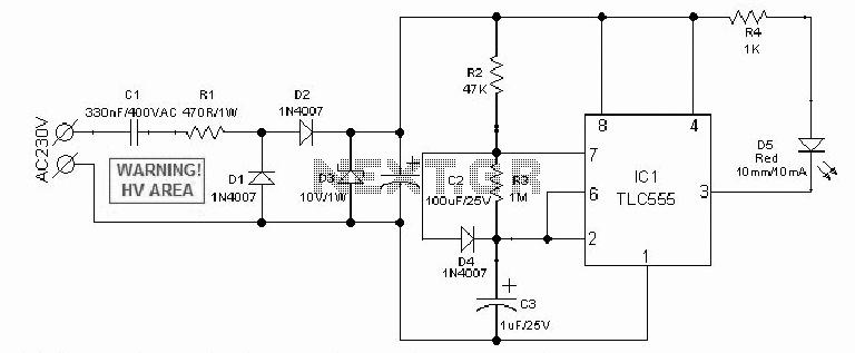
An AC mains operated single LED flasher circuit is designed using the widely used CMOS timer chip TLC555. The entire circuit is powered directly by the grid supply of 230VAC through a capacitive potential divider and associated components. This LED...