
For differential drive circuit diagram of a voltage output DAC AD5620

The circuit configuration in Figure 1 is designed to convert digital signals into analog voltages with precision and stability. The use of the AD5620 DAC allows for a high-resolution output, which is essential for applications requiring accurate signal representation. The control of the DAC through an SPI interface facilitates straightforward integration with microcontrollers or digital signal processors, enabling efficient data transfer and command execution.
The reference voltage of +2.5 V plays a critical role in maintaining the accuracy of the output signal. With a temperature coefficient of 5 ppm/°C, the reference voltage source ensures minimal drift over temperature variations, which is vital for applications in environments with fluctuating temperatures. The common-mode voltage of +2.5 V at the V-side output allows for optimal operation of the AD8042 differential driver, which is designed to amplify the differential signal while rejecting common-mode noise.
The feedback network associated with U2-B is crucial in determining the gain and phase characteristics of the circuit. By forcing a 180-degree phase shift at the V+ terminal, the circuit can effectively manage the output characteristics, ensuring that the signal integrity is preserved. This phase manipulation is particularly important in differential signaling applications, where maintaining the correct timing and phase relationships between signals is critical for performance.
Overall, the circuit depicted in Figure 1 represents a robust solution for generating precise analog outputs from digital inputs, suitable for a wide range of electronic applications. The careful selection of components and configuration ensures high performance and reliability in signal processing tasks.Figure 1 circuit uses a single +V power supply, and a voltage output DAC AD5620. DAC input by an SPI port control. DAC output swing from V to +5 V. Within the DAC chip referenc e voltage source (+2.5 V) to set the AD8042 differential driver circuit common-mode voltage. The temperature coefficient of the reference voltage source is 5 ppm/C. V -Side output common-mode voltage of +2.V is centered inverted DAC output. U2-B feedback network and forcing V + terminal voltage V Terminal voltage phase by 180. Figure 1. Voltage Output DAC AD5620 differential driver
Related Circuits
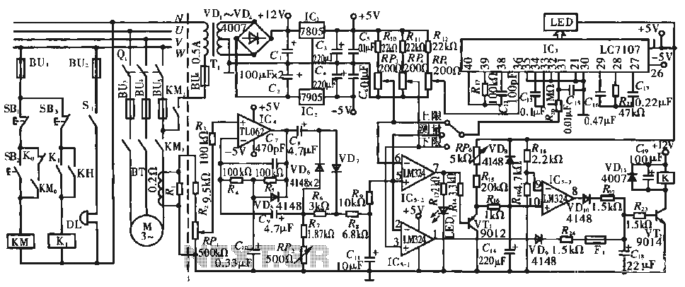
The circuit operates during standard inspection work by utilizing the voltage across resistor R2, which is connected to RP, to generate the input signal for IC4. Components R3 through Rg, along with capacitors C7 and C1, and diodes VD7...

The ISL6315 two-phase PWM control integrated circuit (IC) offers a precise voltage regulation system capable of handling advanced loads ranging from 60A to 80A. Multiphase power conversion represents a significant shift from traditional single-phase converter configurations, which are increasingly...
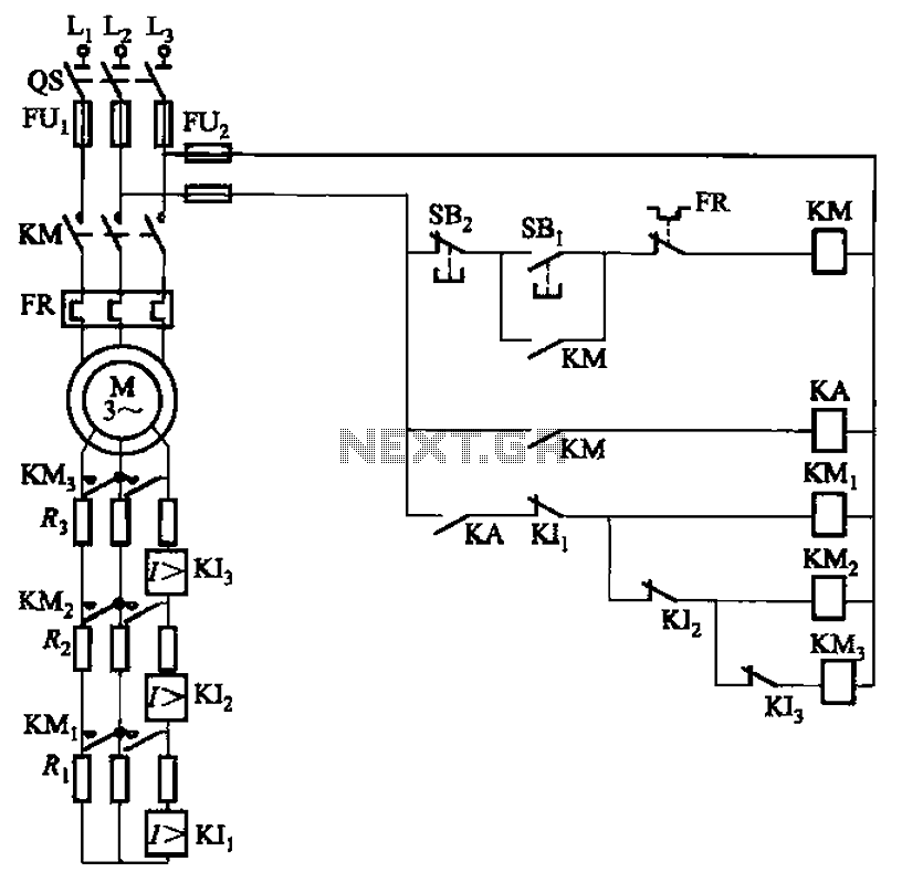
The circuit illustrated in Figure 3-161 features a first stage current detection mechanism utilizing a current relay (KI1) in series with a resistor (R1). The second stage employs another current relay (KI2) in series with a resistor (R2) for...

This circuit utilizes a synchronous demodulator to extract a 1 kHz signal from noise and measures its amplitude, with the 1 kHz signal providing a resolution of approximately 60 microvolts per count. The measurements are transmitted via an RS-232...
The core component of this controller is a switch mode voltage converter. L1 is responsible for converting voltage, while Q1 acts as the switch that controls the current flowing through L1. The switch mode voltage converter operates by rapidly switching...

The circuit is capable of driving the company's Dialight 745-0005 monitor, which features a 64-character alphanumeric display. It generates 0-second and 1-second input signals on lines A1 through A6 based on the phase response of the desired characters, utilizing...