
For driving the power supply circuit of the sensor bridge

The circuit design features a maximum input voltage specification of 10V, which is critical for ensuring the safety and functionality of the operational amplifier (op-amp) employed in the circuit. The reference voltage of 10V is generated through the op-amp, which operates in conjunction with a temperature-compensated Zener diode (IS2192). The Zener diode is selected for its stability across varying temperatures, which is essential for maintaining a consistent output voltage.
The Zener voltage (Vz) can be fine-tuned via a variable resistor, allowing for precise adjustments to counteract any discrepancies that may arise during operation. This variable resistor is crucial for calibrating the circuit to achieve the desired performance specifications. A resistor divider circuit, consisting of resistors R4 and R1, is implemented to facilitate the switching of input voltage levels to the op-amp. This configuration is designed to provide a descending order of input voltages, which can be beneficial for applications requiring varying voltage levels.
To ensure sustained voltage accuracy over time, it is imperative to select resistances that exhibit minimal variation. The recommended range for these resistances is between 0.5 to 10 ohms, which helps to mitigate the effects of drift and enhances the reliability of the circuit.
The circuit incorporates an op-amp buffer amplifier with a gain of 1, which serves to isolate the input from the output, thereby preventing loading effects that could compromise performance. The buffer amplifier is configured positively, ensuring that the output voltage remains in phase with the input voltage. Furthermore, an inverting amplifier configuration is employed to produce a negative voltage output from the circuit. This is achieved by utilizing feedback through a resistor network, which allows for the inversion of the output voltage while maintaining accuracy.
To address potential resistance errors, a variable resistor is included in the design. This component allows for real-time adjustments, facilitating the correction of any inaccuracies in the voltage output. The implementation of these design elements collectively ensures that the circuit operates efficiently, providing stable and precise voltage references as required for various electronic applications.A. The maximum input voltage of 10V. OP amplifier A, to give ten of 10V reference voltage, and its stability is mainly determined by the Zener diode characteristics, mining com mission temperature compensated zener diode (IS2192). Zener voltage Vz if the error can be used to adjust the variable resistor, it is IO. oov. s resistor divider circuit (R4vR,) to switch A, input voltage, ul/2 office units in descending order. When you need to 1 voltage accuracy over time, EU resistance must choose a small difference in disrespect of the product ( 0.5 ~ .10 {).
OP/Ze buffer amplifier 4. The amplifier, save magnification is 1, is positive to put large, but with sleep} line inverting amplifier, the output voltage into a negative voltage inverter output voltage. - said that the resistance r, four errors on a variable resistor r z mouth into line correction, accurate voltage can be obtained.
Related Circuits

A simple FM stereo decoder circuit utilizing the MC1310P integrated circuit (IC). It operates at 12V and provides a channel separation of 40dB, making it suitable for stereo FM receivers. The FM stereo decoder circuit based on the MC1310P IC...
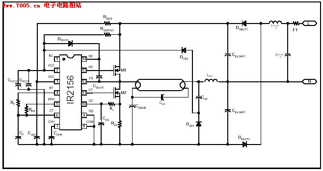
The IR2156 provides a cost-effective solution for fluorescent electronic ballasts. It integrates features such as lighting tube error protection and a programmable working frequency, which includes warm-up, lighting, and continuous operation of the ballast. The IR2156 is a highly integrated...
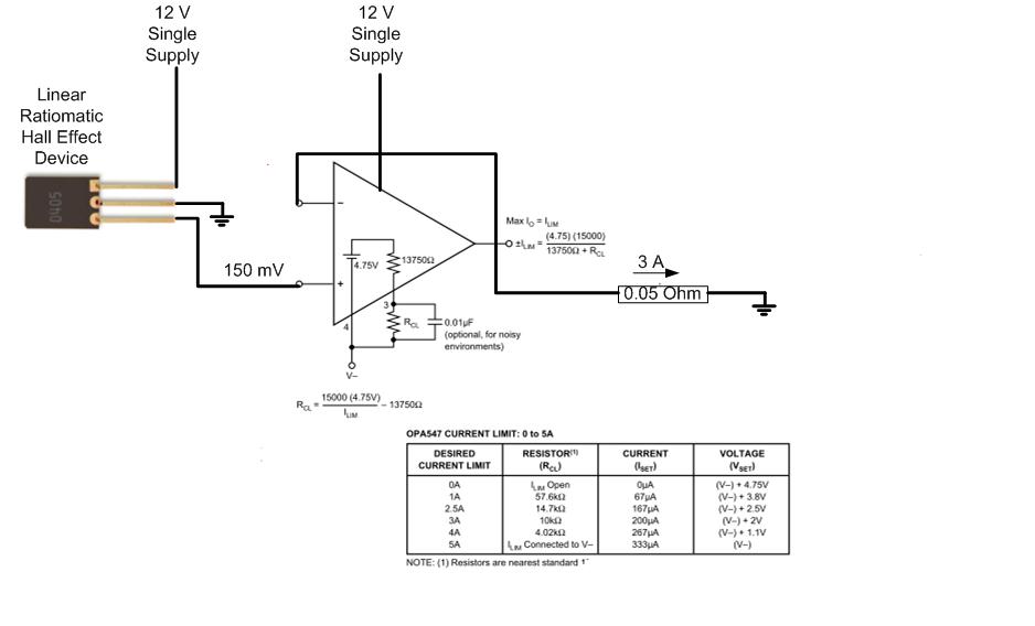
The proposed approach would dissipate (12V)(3A) = 36 watts, which results in significant heat generation in the circuit. This necessitates consideration of two alternatives: 1) Operating the op-amp at a lower supply voltage, if feasible, or 2) Utilizing a...
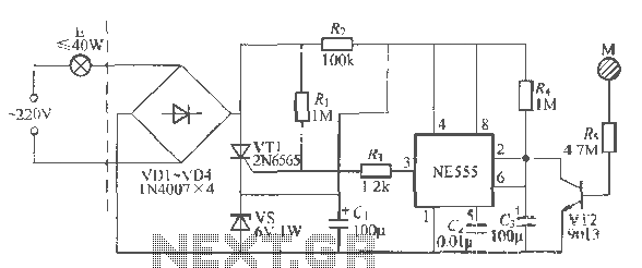
Using a wire connection, utilize the NFA.55 timebase circuit delay type light touch switch, which can directly replace an ordinary mechanical switch without needing to modify the original internal wiring. The circuit is powered back with good hoof Chapter...
As the position of the sun changes, the illumination level on the light-dependent resistors (LDRs) also varies, causing the input voltage for the window comparator to deviate from half of the supply voltage. Consequently, the output of the comparator...

Basic features include an internal 512k-bit EEPROM, allowing for continuous recording and playback at any time, with long-term retention of voice data after power loss. The voice recording time is 20 seconds, and it supports segmented recording and playback....