
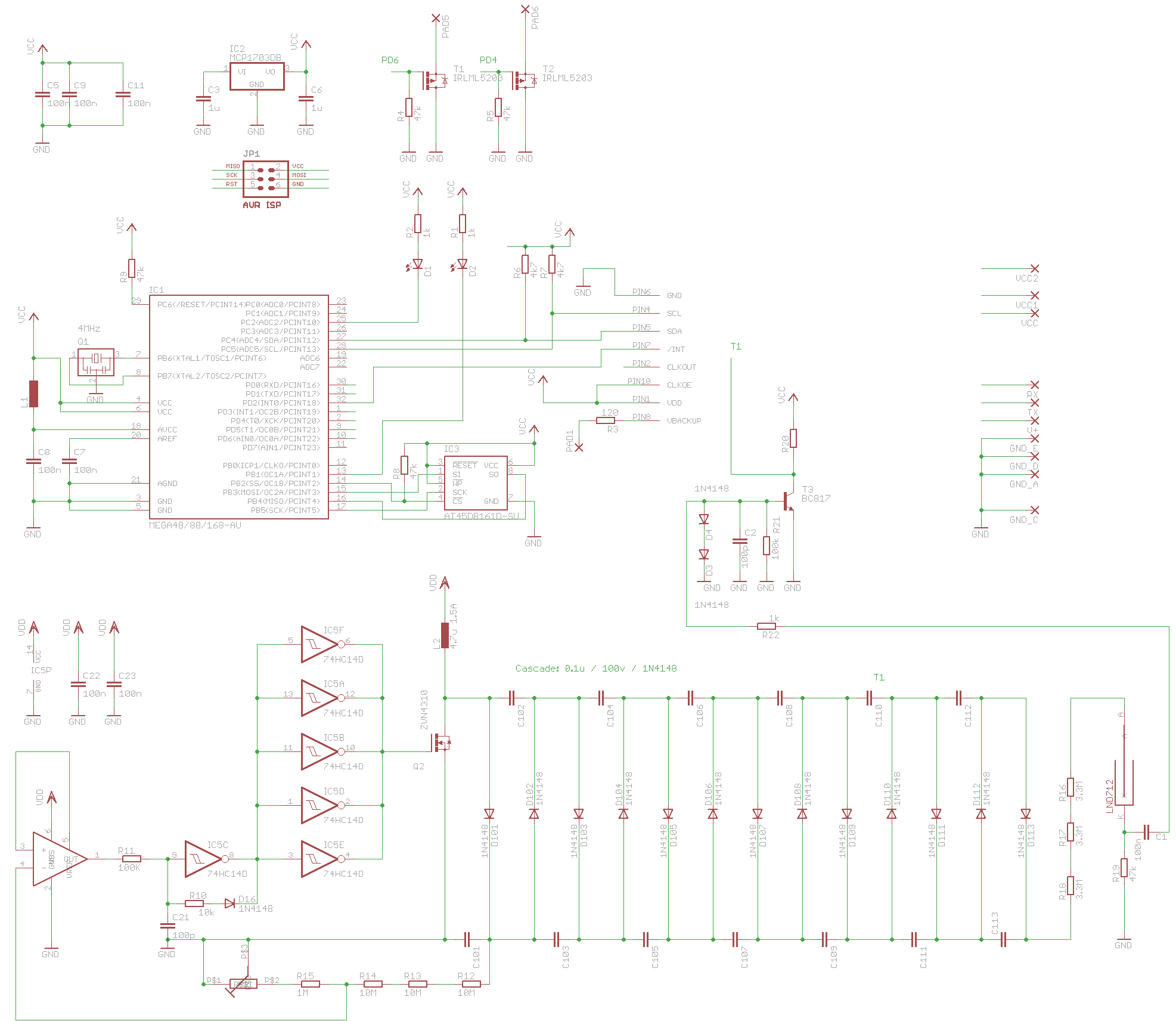
Frequency counter hardware keys schematic

The circuit design incorporates four debounced switches that enhance user interaction by preventing erroneous signals caused by mechanical bounce. Each switch is connected to a Schmitt trigger, which is essential for converting the noisy signal from the switch into a clean digital signal suitable for further processing. The combination of resistors and capacitors at the input of the Schmitt triggers forms an RC debouncing network, effectively filtering out transient fluctuations that occur when the switch is actuated.
The output of each Schmitt trigger is connected to a D-type flip-flop, which serves as a memory element in the circuit. The flip-flop changes its output state in response to the clock signal generated by the switch press, thereby allowing for a stable representation of the button's state. This toggling behavior is critical for applications that require reliable state changes based on user input.
Each switch is also paired with an LED indicator, providing visual feedback to the user. The use of standard LEDs for some switches and bidirectional two-color LEDs for others allows for a versatile user interface, where different colors can indicate different states or actions.
To monitor whether any key has been pressed, a diode logic circuit is employed. This circuit aggregates the outputs from the switches and generates a single signal that indicates any button press, enhancing the functionality of the logic board. However, it is important to note that this feature does not apply to the "hold" key located in the top-right position.
To ensure that the flip-flops start in a known state when the device is powered on, a reset logic circuit is implemented using IC3E. This circuit guarantees that all flip-flops are initialized correctly, preventing any unpredictable behavior during startup.
The time constant of the debouncing circuit is defined by the values of resistor R8 and capacitor C7. This time constant is crucial as it determines how quickly the circuit responds to switch activations and how effectively it filters out noise, ensuring that the system remains responsive while maintaining stability in the output signals. Overall, this circuit design effectively combines user interface elements with robust signal processing to create a reliable and user-friendly electronic system.This is basically 4 nearly identical debounced switches. The 2 resistors and one capacity at the input of each Schmitt trigger are used for debouncing the switches. The output is then fed into a D-type flip-flop which uses feedback to change the state (LOW to HIGH, HIGH to LOW) each time the button is pressed.
Each key has a LED indicator, two wit h simple LEDs and two with bidirectional 2-color LEDs. A simple "diode logic" circuit is used for the "any key pressed" signal (which is not used for the right-top "hold" key) to be able to make the logic board aware that buttons were pressed. IC3E forms a simple reset logic which makes sure that all the flip-flops are in proper state when the device is switched on.
The time constant is determined by R8 and C7. 🔗 External reference
Related Circuits
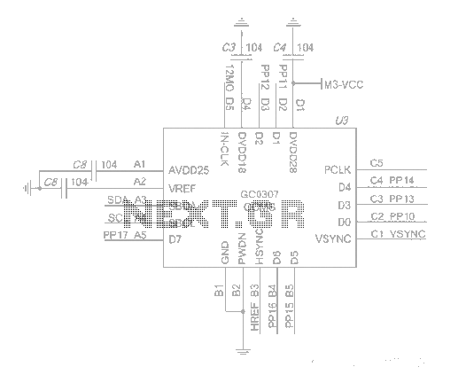
The system employs an optical fingerprint sensor utilizing the ARM Cortex M3 core, specifically the STMicroelectronics 32-bit high-performance microcontroller STM32F205RE. It incorporates a function body composition that utilizes the Sobel edge detection operator, Gabor filtering, image binarization, and various...
This circuit is designed for radiation logging purposes. It is based on an Atmel 168 Microcontroller and a precise RTC device called RV3029. An AT45DB41 Dataflash is utilized in this circuit, leveraging pre-existing source code for communication with this...
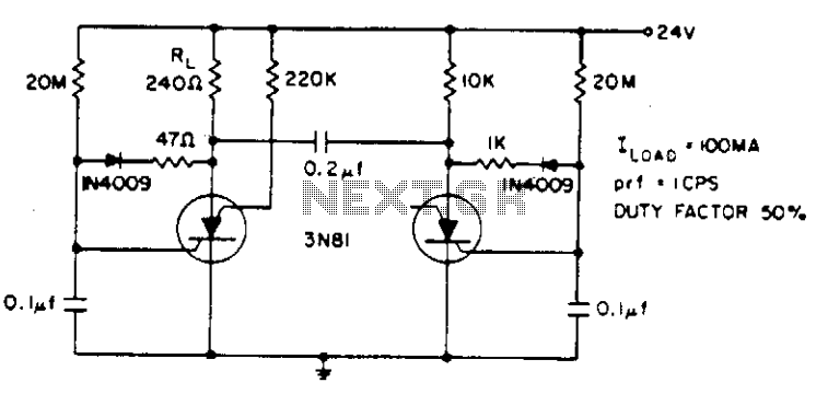
Electrolytic capacitors are not required to generate a 1 cps frequency. When the silicon-controlled switch (SCS) is triggered, the 0.2 µF commutating capacitor deactivates the other capacitor and charges its gate capacitor to a negative potential. The gate capacitor...

The circuit utilizes a dual operational amplifier integrated circuit (IC), specifically the 1458, which contains two separate op-amps within a single package. In this configuration, the first op-amp functions as a voltage follower, directing its output to charge capacitor...
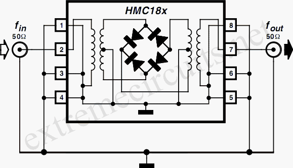
When working with frequencies ranging from 850 MHz to 4 GHz, a frequency multiplier may be necessary. The HMC 187, HMC 188, and HMC 189 frequency doublers could be suitable solutions. These devices offer isolation performance that attenuates the...
The following diagram illustrates a four-band blaster circuit. This blaster is utilized to enhance sound fidelity, emphasize specific instruments, eliminate unwanted noise, or create entirely new and distinct timbres. The four-band blaster circuit is designed to manipulate audio signals across...