
Frequency tripler

The primary function of this circuit is to utilize the switching characteristics of complementary transistors, typically a PNP and an NPN transistor, to achieve frequency tripling. The design leverages the unique turn-on and turn-off behavior of the transistors to manipulate the input waveform effectively. When a periodic signal is applied, the transistors alternately saturate and cut off, resulting in the generation of additional peaks in the output waveform.
The circuit can be visualized as having an input stage where the periodic waveform is fed into the base terminals of the transistors. As the input signal rises, one transistor turns on while the other turns off, allowing current to flow through the collector-emitter path. This action creates a corresponding output peak. When the input signal reaches a certain threshold, the first transistor saturates, causing the second transistor to turn on, which generates the second output peak. This process continues, resulting in the tripling of the frequency of the original input signal.
The output waveform will contain three distinct peaks for every cycle of the input waveform, effectively tripling the frequency. However, the circuit's performance may be compromised by the asymmetry of the output peaks, which can lead to distortion in the final signal. This lack of symmetry arises from the inherent differences in the turn-on and turn-off times of the complementary transistors, which can be influenced by factors such as transistor characteristics and circuit design.
This circuit's operational frequency range extends from DC up to the maximum frequency that the selected complementary transistor pair can handle, making it versatile for various applications in signal processing. The design can be further optimized by selecting transistors with matched characteristics to minimize output asymmetry and improve overall performance.The turn-on and turn-off characteristics of two complementary transistors can be combined to attain nonselective frequency tripling. The resulting circuit handles any periodic waveform with nonvertical sides. Each input signal peak produces three output signal peaks. The additional peaks occur where the input signal causes saturation of one of the two transistors. The circuit operates over a frequency range from dc to the upper limits of the complementary transistor pair.
About the only disadvantage of the circuit is the lack of symmetry of the output signal peaks.
Related Circuits
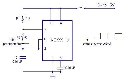
A NE555 integrated circuit (IC) is utilized for the design of a variable low-frequency oscillator, and a schematic is provided. The NE555 timer IC is a versatile and widely used device in various electronic applications, particularly in generating precise timing...
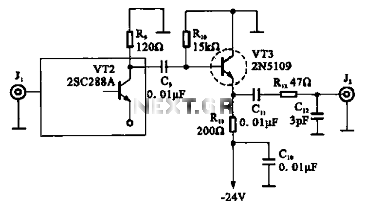
A high-frequency signal is displayed in the output amplifier. The circuit consists of a VI3 common collector amplifier (emitter follower) designed to enhance the child-band. It is a high-frequency amplifier (1-250 MHz) that increases the output voltage and boosts...

The circuit was designed to create an electronic oscillator known as the Wien Bridge Oscillator, which can be used for the generation of low-frequency sine waves. The Wien Bridge Oscillator is a type of electronic oscillator that generates sine waves....
The SE555/NE555 timer was first introduced by Signetics Corporation around 1971. The pin connections and their functions are as follows: Pin 1 (Ground) is the most-negative supply potential and is typically connected to circuit common when powered by positive...

Bass and midrange frequencies are significantly influenced by Marshall's considerable adjustment of R1 and are somewhat affected by the 10-percent increase in C2 and C3. The following paragraphs will explain how the circuit responds to bass and midrange frequencies,...
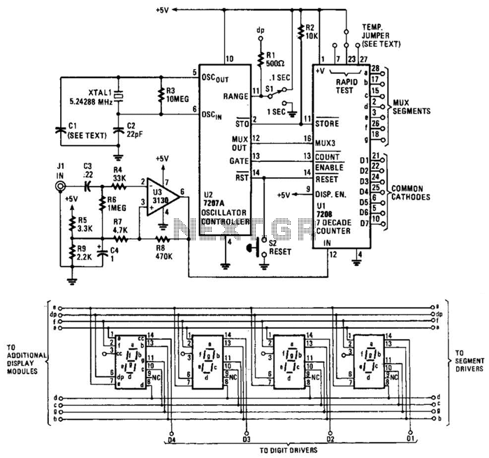
The circuit comprises an ICM7208 seven-decade counter (U1), an ICM7207A oscillator controller (U2), and a CA3130 biFET operational amplifier (U3). Integrated circuit U1 counts input signals, decodes them into a 7-segment format, and outputs signals to drive a 7-digit...